Row decoding circuit and memory

a decoding circuit and memory technology, applied in the field of memory technology, can solve problems such as reducing storage density, and achieve the effect of enhancing driving voltage and driving speed of memory array

Active Publication Date: 2015-07-14
SHANGHAI HUAHONG GRACE SEMICON MFG CORP
View PDF3 Cites 3 Cited by
  • Summary
  • Abstract
  • Description
  • Claims
  • Application Information

AI Technical Summary

Benefits of technology

[0023]Compared with the prior art, the present disclosure has the following advantages:
[0024]By detecting the voltage of the first dummy control-gate line voltage output and the voltage of the second dummy control-gate line voltage output of the dummy row decoding unit, the third driving voltage, which is used to drive the first control-gate line voltage output and the second control-gate line voltage output of the row decoding unit, is controlled. Thus, in an initial stage, the first voltage is used to drive the first control-gate line voltage output and the second control-gate line voltage output. After voltage of any one of the first dummy control-gate line voltage output and the second dummy control-gate line voltage output is detected to rise to a predetermined voltage, the second voltage is used to drive the first control-gate line voltage output and the second control-gate line voltage output. The first voltage is greater than the second voltage. The driving speed of the memory array is enhanced by using the first voltage to drive the first control-gate line voltage output and the second control-gate line voltage output. Due to the enhancement of the driving voltage, the area of the driving transistor in the control-gate line driving unit of the row decoding unit is reduced.

Problems solved by technology

However, the memory units of flash memory having a relatively large area may reduce the storage density.

Method used


Image

  • Row decoding circuit and memory
  • Row decoding circuit and memory
  • Row decoding circuit and memory

Examples


Embodiment Construction

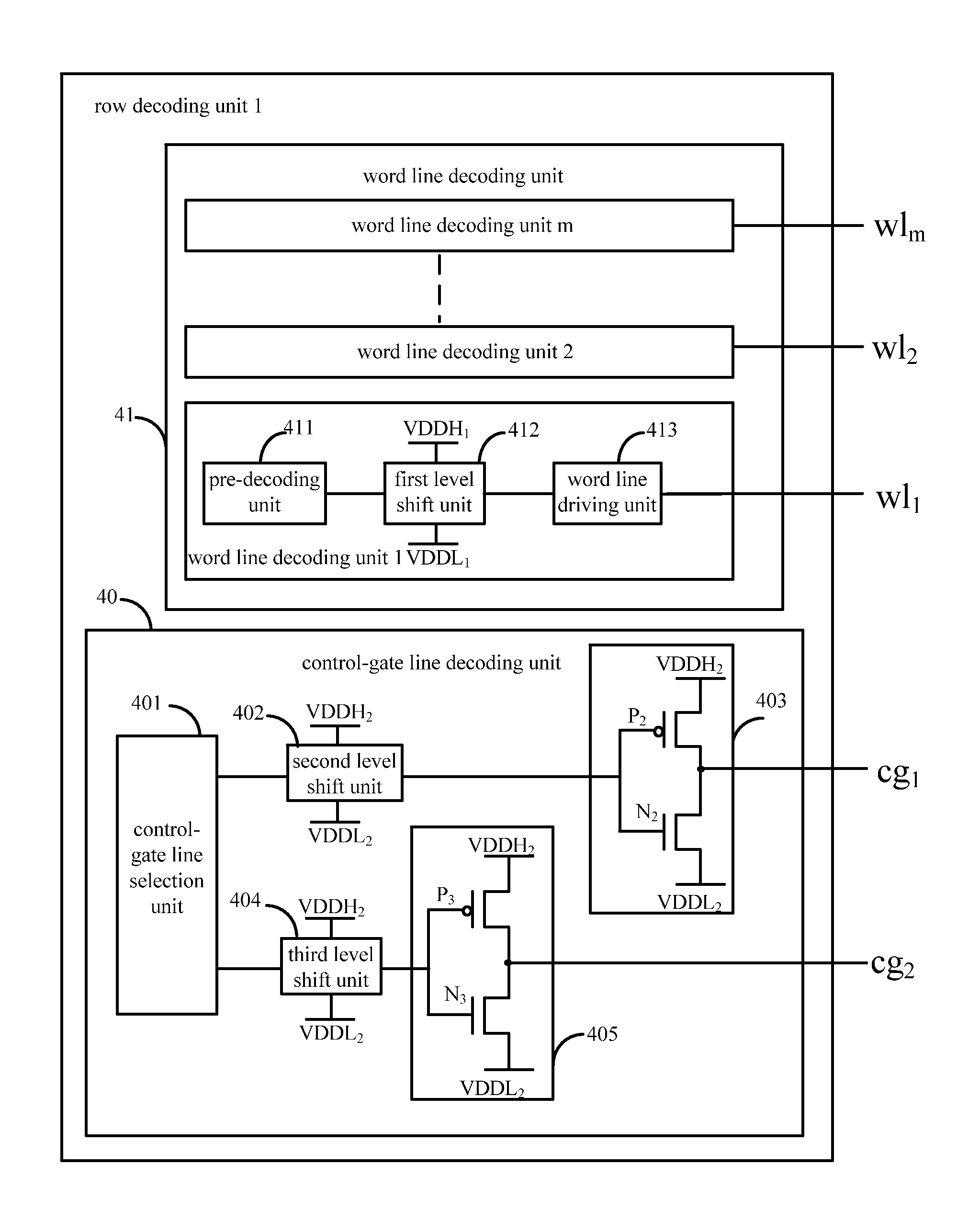
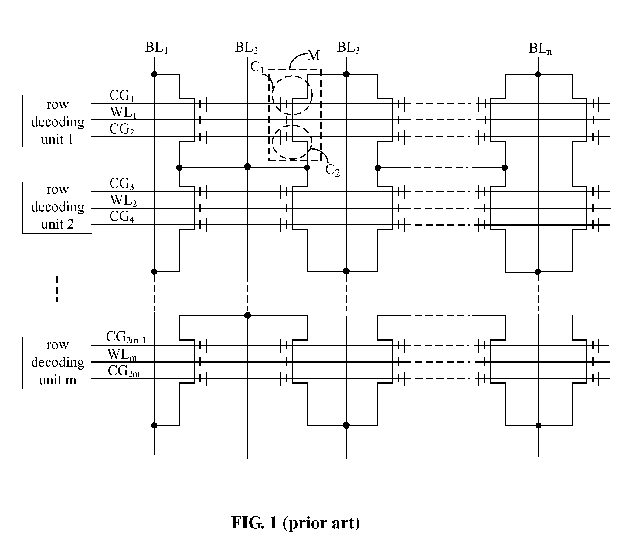
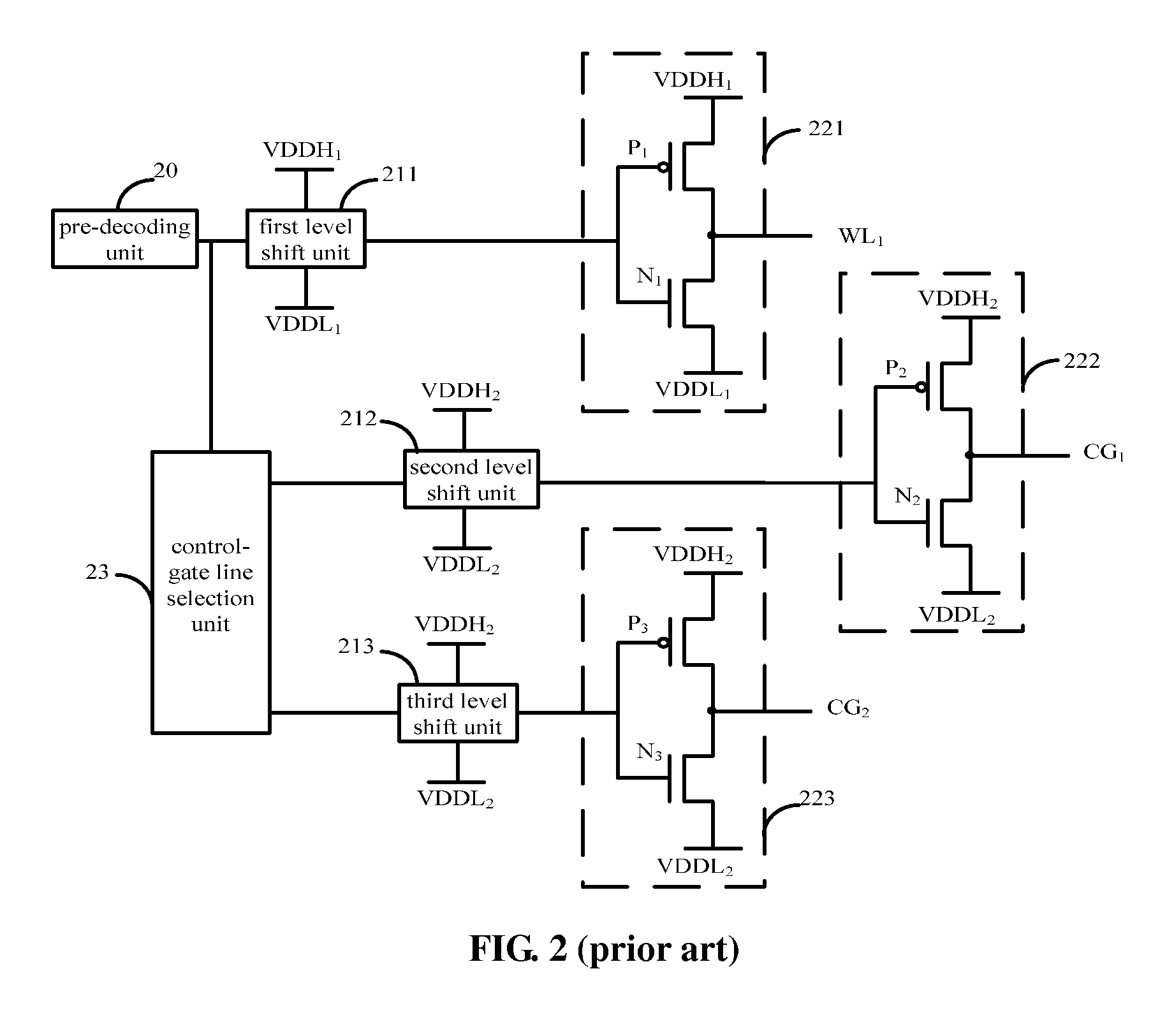
[0032]As described in the background, the row decoding circuit of a conventional dual-bit split gate flash memory array includes a plurality of row decoding units. Each row decoding unit corresponds to a row of memory units, and provides a word line operation voltage and a control-gate line operation voltage to the memory units. The conventional row decoding circuit occupies a large chip area. In addition, the area of driving transistors in each row decoding unit is reduced in order to reduce the area of the row decoding circuit, which may slow down the driving speed of the memory array. Therefore, a row decoding circuit with a high speed and a small area is provided in this disclosure based on the inventors' research.

[0033]In order to clarify the objects, characteristics and advantages of the disclosure, the embodiments of the present disclosure will be described in detail in conjunction with the accompanying drawings.

[0034]The disclosure will be described with reference to certain...


PUM


Abstract

A row decoding circuit and a memory are provided. The row decoding circuit is adapted for providing a word line operation voltage and a control-gate line operation voltage to a dual-bit split gate flash memory array, and includes a dummy row decoding unit, at least one row decoding unit and a driving voltage generating circuit. The dummy row decoding unit includes a first dummy control-gate line voltage output, a second dummy control-gate line voltage output and at least one dummy word line voltage output. The row decoding unit includes a first control-gate line voltage output, a second control-gate line voltage output and at least one word line voltage output. The driving voltage generating circuit is adapted for providing a third driving voltage to the first control-gate line voltage output and the second control-gate line voltage output.

Description

CROSS-REFERENCE TO RELATED APPLICATIONS[0001]The present application claims priority to Chinese patent application No. 201210564385.5, filed on Dec. 21, 2012, and entitled “ROW DECODING CIRCUIT AND MEMORY”, the entire disclosure of which is incorporated herein by reference.TECHNICAL FIELD[0002]The present disclosure generally relates to memory technology, and more particularly, to a row decoding circuit and a memory.BACKGROUND[0003]As an integrated circuit memory device, a flash memory has a function of storing information which is electrically erasable. Therefore, flash memory is widely used in electronic products, such as laptops, mobile phones, digital music players and etc. According to different gate structures, flash memories are generally classified into two types: stacked-gate flash memories and split-gate flash memories, in which memory units are required to be arranged in an array for proper operation and each memory unit is used to store a single bit of data. In such a me...

Claims


Application Information

Patent Timeline
Patent Type & Authority Patents(United States)
IPC IPC(8): G11C7/00G11C8/08G11C16/04G11C16/08
CPCG11C16/08G11C8/08G11C16/0433G11C8/10
Inventor YANG, GUANGJUN
Owner SHANGHAI HUAHONG GRACE SEMICON MFG CORP
Why Eureka
Try Eureka