Semiconductor device

Inactive Publication Date: 2016-08-25
SHARP KK
View PDF0 Cites 13 Cited by
  • Summary
  • Abstract
  • Description
  • Claims
  • Application Information

AI Technical Summary

Benefits of technology

[0044]According to an embodiment of the present invention, in a semiconductor device which includes a memory transistor and a plurality of select transistors, it is possible to suppress deterioration of the characteristics of a select transistor which is present in

Problems solved by technology

In this memory transistor, the metal oxide semiconductor is a resistor after

Method used


Image

  • Semiconductor device
  • Semiconductor device
  • Semiconductor device

Examples


first embodiment

[0093]The first embodiment of the semiconductor device of the present invention is a nonvolatile semiconductor storage device including a plurality of memory cells arranged in row and column directions (hereinafter, referred to as “nonvolatile memory array”). The memory cells include a memory transistor and a plurality of select transistors.

[0094](Configuration of Memory Cell 101)

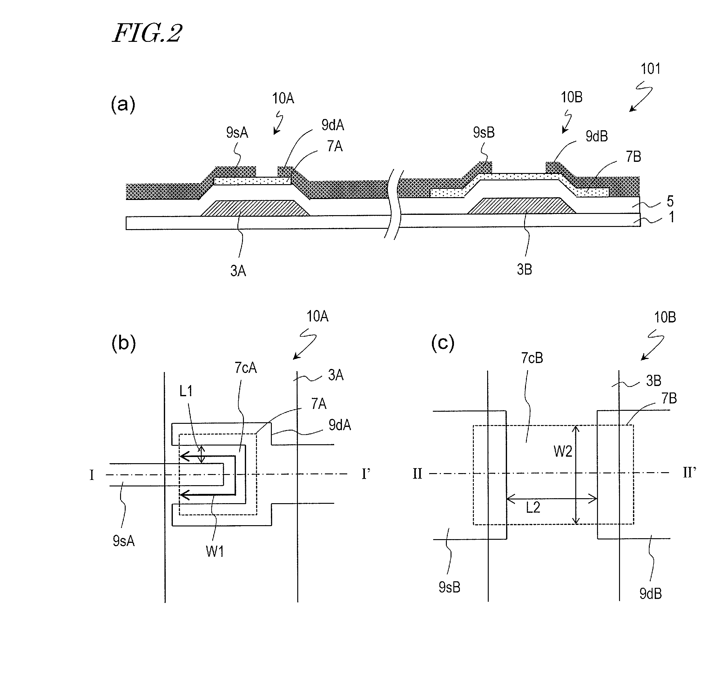
[0095]FIG. 2(a) is a cross-sectional view showing a memory transistor 10A and a select transistor 10B in a memory cell 101 of the present embodiment. FIGS. 2(b) and 2(c) are plan views of the memory transistor 10A and the select transistor 10B, respectively. FIG. 2(a) shows cross-sectional structures taken along line I-I′ of FIG. 2(b) and line II-II′ of FIG. 2(c).

[0096]The memory cell 101 includes a substrate 1, a memory transistor 10A supported on the substrate 1, and a plurality of select transistors 10B each supported on the substrate 1. These transistors 10A, 10B have active layers (oxide semiconductor ...

second embodiment

[0196]The second embodiment is described with reference to FIG. 14.

[0197]FIG. 14 shows a configuration example of a nonvolatile memory array 2001 in which a plurality of memory cells 101 are arranged in a row direction. In the nonvolatile memory array 2001 of the present embodiment, the memory cells 101 have the same configuration as that of the memory cell 101 shown in FIG. 3(a). A single memory cell 101 is arranged only in a row direction. The other components are the same as those of the nonvolatile memory array 1001 of the first embodiment. Therefore, detailed descriptions of the respective components are omitted.

[0198]Now, typical examples of writing and reading operations of the nonvolatile memory array 2001 are described.

[0199]During writing, the bit line decoder 103 applies writing voltage Vpp to the bit line BLn of a selected memory cell 101. The word line decoder 104 and the writing voltage control circuit 105 apply a voltage which is at the same level as writing voltage V...

third embodiment

[0205]The third embodiment is described with reference to FIG. 15.

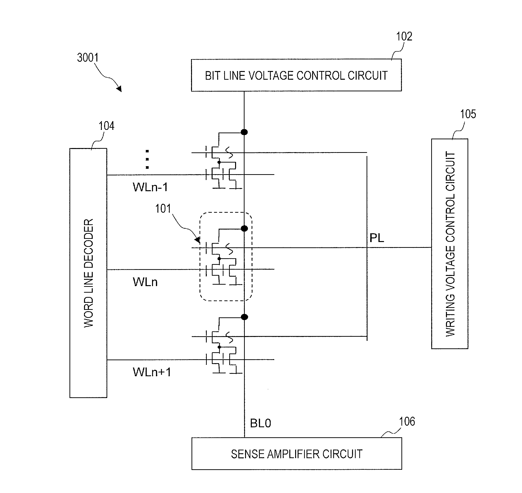
[0206]FIG. 15 shows a configuration example of a nonvolatile memory array 3001 in which a plurality of memory cells 101 are arranged in a column direction. In the nonvolatile memory array 3001 of the present embodiment, the memory cells 101 have the same configuration as that of the memory cell 101 shown in FIG. 3(a). k memory cells 101 are arranged only in a column direction. The gate electrodes of the memory transistors 10A included in the memory cells 101 are connected with the writing voltage control circuit 105 via a common word line PL. The other components, except for the bit line decoder, are the same as those of the nonvolatile memory array 1001 of the first embodiment. Therefore, detailed descriptions of the respective components are omitted. The reason for the absence of the bit line decoder is that only one bit line BL is provided. It is not necessary to select a specific bit line BLn from a plurality of b...


PUM


Abstract

A memory cell (101) includes a memory transistor (10A) having channel length L1 and channel width W1, and a plurality of select transistors (10B) each electrically being connected in series with the memory transistor and independently having channel length L2 and channel width W2, wherein each of the memory transistor and the plurality of select transistors includes an active layer (7A) formed from a common oxide semiconductor film, the memory transistor is a transistor which is capable of being irreversibly changed from a semiconductor state where drain current Ids depends on gate voltage Vg to a resistor state where drain current Ids does not depend on gate voltage Vg, and channel length L2 is greater than channel length L1.

Description

TECHNICAL FIELD[0001]The present invention relates to a semiconductor device and particularly to a semiconductor device which includes a memory transistor and a select transistor.BACKGROUND ART[0002]Using an element which has a transistor structure as a memory element which can be used as a ROM (Read Only Memory) has been conventionally proposed.[0003]For example, Patent Document 1 discloses an eFuse (Electronic Fuse) in which two terminals, a cathode and an anode, are provided in a multilayer structure of polysilicon / silicide / silicon nitride film, which has the same wire structure as that used in common logic LSI processes. By allowing a large electric current to flow through this eFuse, the eFuse is heated, and the resistance value between the two terminals varies. Although Patent Document 1 fails to disclose the technique of using the eFuse as a memory cell, Patent Document 1 discloses a configuration where two transistors (select transistors) and an eFuse are connected in series...

Claims


Application Information

Patent Timeline
IPC IPC(8): G11C17/16H01L29/10H01L27/112H01L29/786H01L29/423G11C17/18H01L29/24
CPCH01L27/101H01L29/7869G11C17/16G11C17/18H01L27/11206H01L29/1033G11C13/0011G11C13/0004H01L29/24H01L29/42356G11C2213/79G11C13/0002G11C13/003G11C13/004G11C13/0069G11C19/184G11C19/28G11C2213/15G11C2213/53G11C2213/74H10B20/20
Inventor UEDA, NAOKIKATOH, SUMIO
Owner SHARP KK
Why Eureka
Try Eureka