Heating device and semiconductor manufacturing apparatus

a manufacturing apparatus and heating device technology, applied in the direction of heating arrangements of hot plates, heating elements, coatings, etc., can solve the problems of uneven thickness of a film obtained by cvd, degraded temperature control properties, and long time to achieve stable temperature, so as to reduce the number of turns, reduce the density of heating, and increase the temperature of the central portion of the ceramic base.

Active Publication Date: 2015-09-01
NGK INSULATORS LTD
View PDF6 Cites 5 Cited by
  • Summary
  • Abstract
  • Description
  • Claims
  • Application Information

AI Technical Summary

Benefits of technology

[0006]When source gas is introduced immediately after starting a CVD process, the temperature of the central portion of a ceramic base may increase. Accordingly, a temperature distribution may be set in advance so that the temperature is lower in the central portion than in the peripheral portion of the ceramic base. Such a temperature distribution is referred to as a center-cool temperature distribution. For example, in the case where a coil -spring-shaped resistance heating element is used the center-cool temperature distribution can be easily realized by reducing the number of turns of winding in the central portion (i.e., reducing the density of heating in the central portion) relative to the number of turns of winding in the peripheral portion of the ceramic base. Generally, the temperature of the ceramic base is controlled by measuring the temperature of the ceramic base using a thermocouple and controlling power supplied to the resistance heating element so that the measured temperature reaches a predetermined target temperature. In case, the thermocouple is arranged to measure the temperature of the central portion of the base inside (i.e., inside the hollow shaft).

Problems solved by technology

However, the temperature control property is degraded immediately after placing a wafer on a wafer-receiving surface or when heat input from the plasma to a wafer occurs during a CVD process, and it takes a long time until a stable temperature is obtained.
This has posed a problem, such as the thickness of a film obtained by the CVD being uneven.
However, when the temperature of the hollow shaft increases excessively, an O-ring, with which the lower end of the hollow shaft is sealed, may be deteriorated by heat and its sealing property may be degraded.

Method used


Image

  • Heating device and semiconductor manufacturing apparatus
  • Heating device and semiconductor manufacturing apparatus
  • Heating device and semiconductor manufacturing apparatus

Examples


experimental examples 1 to 11

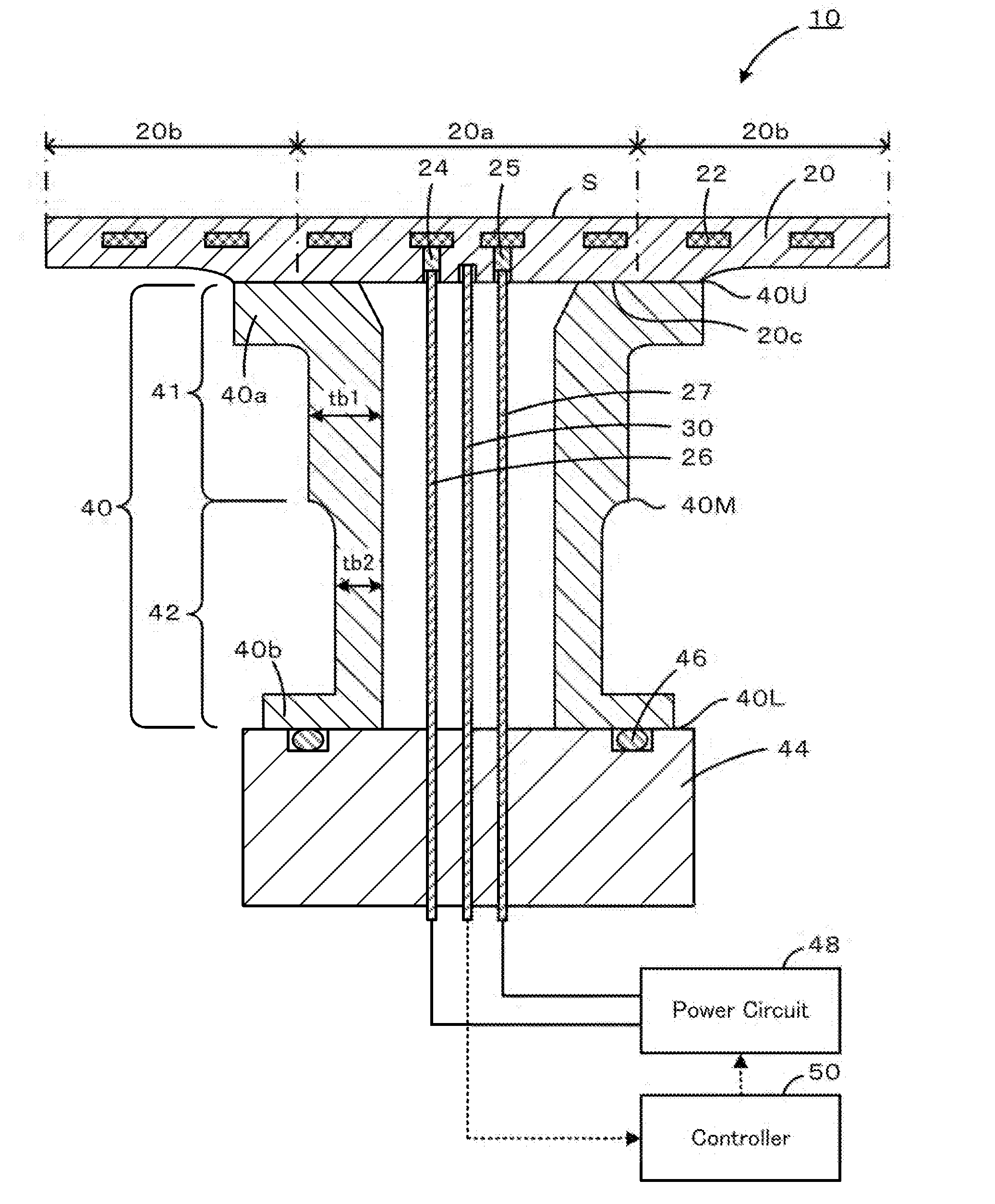
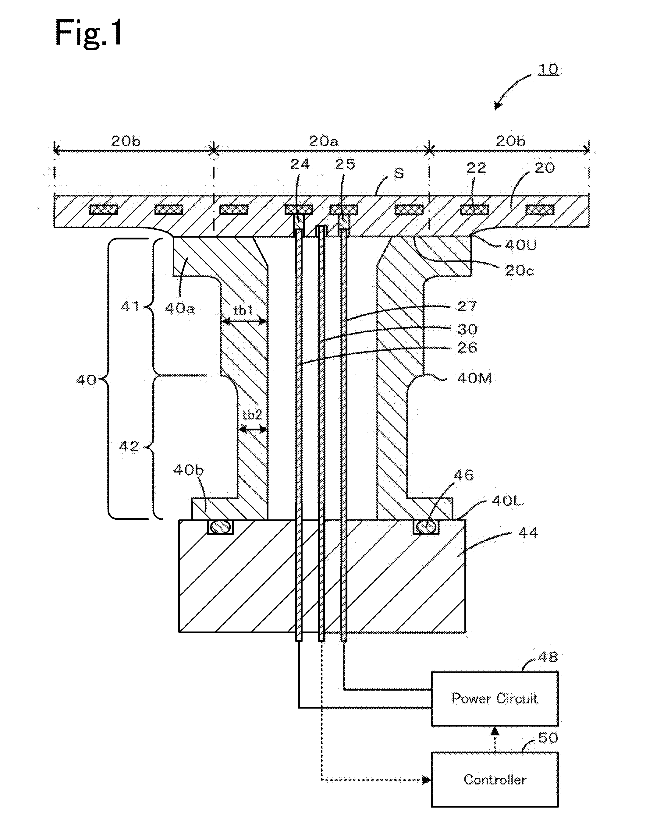
[0049]The heating device 10 shown in FIG. 1 was prepared for each of Experimental examples. FIG. 4 and Table 1 show the dimensions of the heating device 10 of each of Experimental examples. A specific preparation procedure is described below.

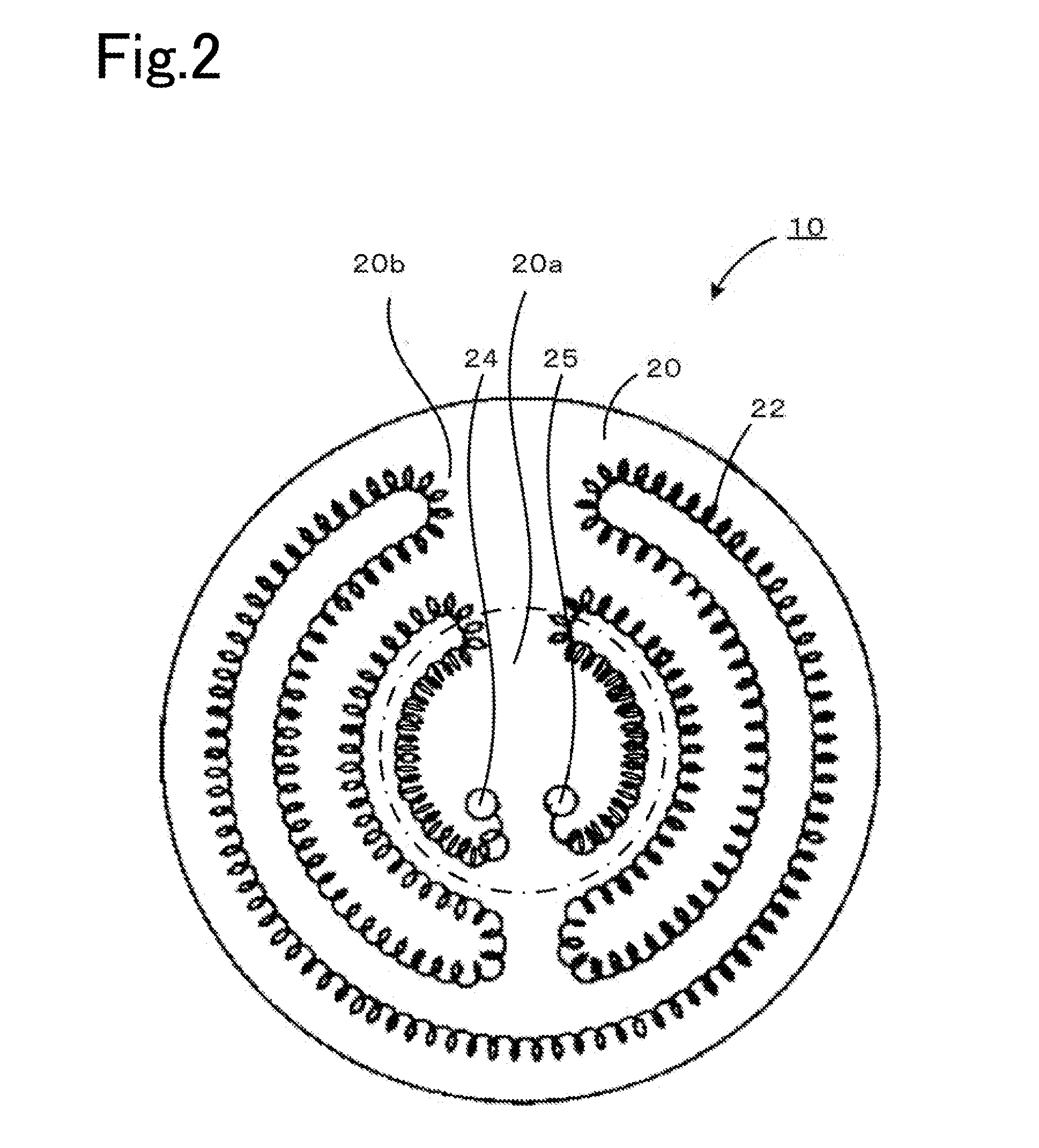
[0050]First, an AlN molded body was prepared. The AlN raw material powder used had a purity of 99%. A resistance heating element constituted by a coil spring composed of Mo was buried in the AlN molded body so as to be distributed throughout the AlN molded body. The resistance heating element was buried in such a manner that the resistance heating element started at a vicinity of the center of the AlN molded body, was arranged over the entirety of the AlN molded body in the manner of a single continuous line, and returned to the vicinity of the center. A positive terminal was attached to an end of the resistance heating element and a negative terminal was attached to the other end of the resistance heating element. The central portion of the AlN...


PUM

PropertyMeasurementUnit
thicknessaaaaaaaaaa
thicknessaaaaaaaaaa
thickness tb1aaaaaaaaaa

Abstract

A heating device 10 includes a ceramic base 20, a resistance heating element 22, and a hollow shaft 40. The ceramic base 20 includes a central portion 20a and a peripheral portion 20b. The resistance heating element 22 is designed in such a manner that the density of heating in the central portion 20a is 1.4 to 2.0 times that in the peripheral portion 20b. The hollow shaft 40 includes a first section 41 and a second section 42. The thickness tb1 of the first section 41 is 6 to 10 mm. The thickness tb2 of the second section 42 is 0.3 to 0.5 times the thickness tb1 of the first section 41. The length of the first section 41 is 0.4 to 0 / 8 times the overall length of the hollow shaft 40.

Description

BACKGROUND OF THE INVENTION[0001]1. Field of the Invention[0002]The present invention relates to a heating device and a semiconductor manufacturing apparatus,[0003]2. Description of the Related Art[0004]To fabricate a semiconductor thin film using source gas, such as silane gas, by thermal CVD, plasma CVD, or the like, a semiconductor manufacturing apparatus employs a heating device for heating a wafer. A known type of heating device includes a disk-shaped ceramic base that has a wafer-receiving surface, a resistance heating element disposed inside or on the surface of the ceramic base, and a hollow shaft attached to the surface opposite to the wafer receiving surface of the ceramic base. Various methods for making the temperature of the wafer-receiving surface of the heating device uniform are known. For example, in the case where a coil-spring-shaped resistance heating element (winding element is buried in the ceramic base, the amount of heat generated per unit area of the wafer-r...

Claims


Application Information

Patent Timeline
Patent Type & Authority Patents(United States)
IPC IPC(8): H05B3/68C23C16/00H01L21/67H05B3/28H05B1/02H01L21/687
CPCH01L21/67103H01L21/68792H05B1/0233H05B3/283H01L21/205H01L21/324
Inventor UNNO, YUTAKAWAKI, JUNYA
Owner NGK INSULATORS LTD
Why Eureka
Try Eureka