Sense amplifier offset voltage reduction

a technology of offset voltage and sense amplifier, applied in the field of characterization and compensation of sense amplifier voltage offset, to achieve the effect of reducing errors, reducing voltage offset, and reducing errors

Active Publication Date: 2015-09-22
QUALCOMM INC
View PDF19 Cites 55 Cited by
  • Summary
  • Abstract
  • Description
  • Claims
  • Application Information

AI Technical Summary

Benefits of technology

[0009]One particular advantage provided by at least one of the disclosed embodiments is a reduction in errors when comparing an output voltage corresponding to a data cell with an output voltage corresponding to a reference cell. For example, a voltage offset of a sense amplifier (e.g., due to process variations during manufacturing) may be removed or reduced. Reducing the voltage offset may result in fewer errors when the sense amplifier compares the output voltage corresponding to the data cell with the output voltage corresponding to the reference cell.

Problems solved by technology

The offset voltage may reduce the sensing margin between the data cell and the reference cell and may thus cause errors when comparing an output voltage corresponding to the data cell with an output voltage corresponding to the reference cell.

Method used


Image

  • Sense amplifier offset voltage reduction
  • Sense amplifier offset voltage reduction
  • Sense amplifier offset voltage reduction

Examples


Embodiment Construction

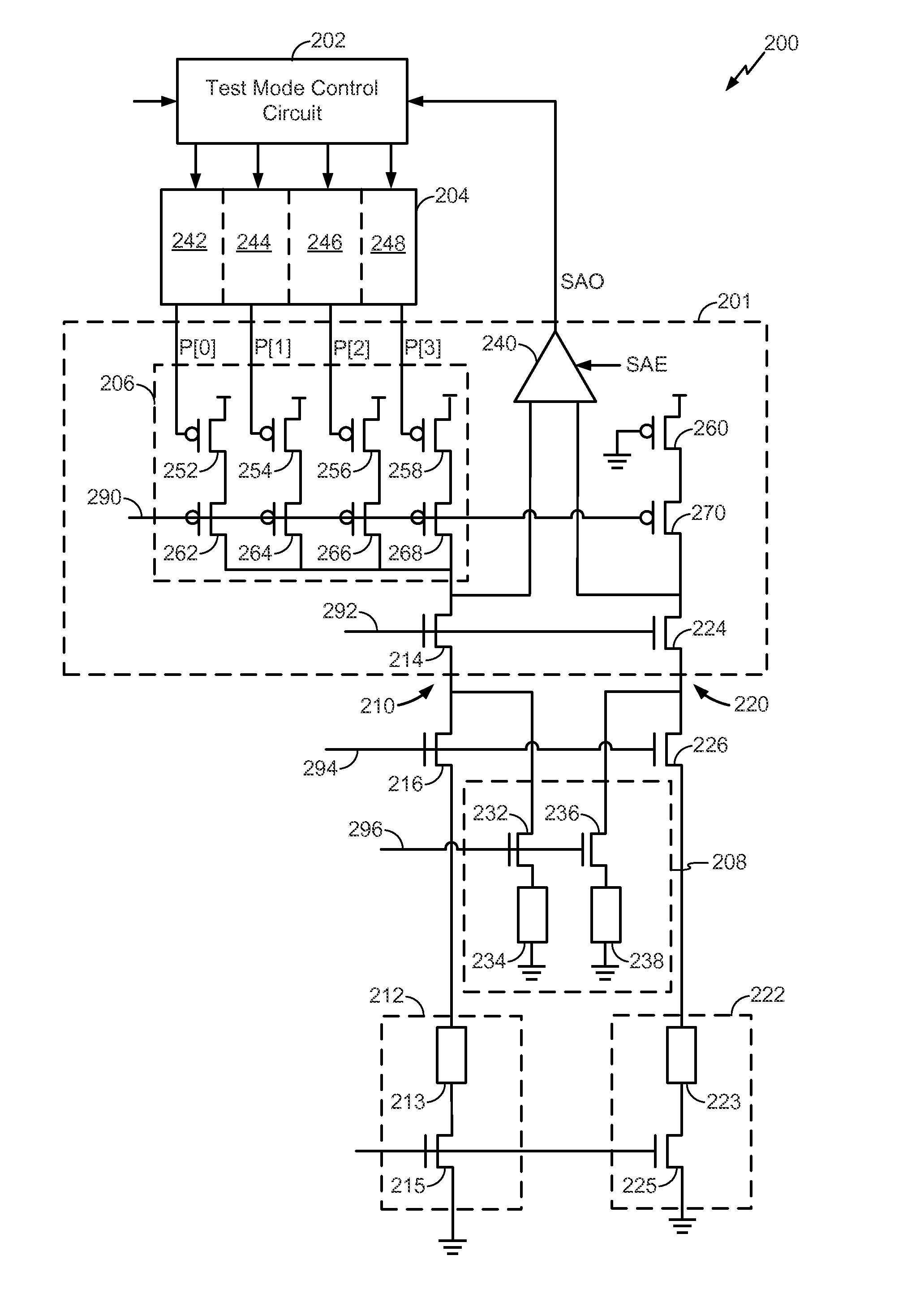
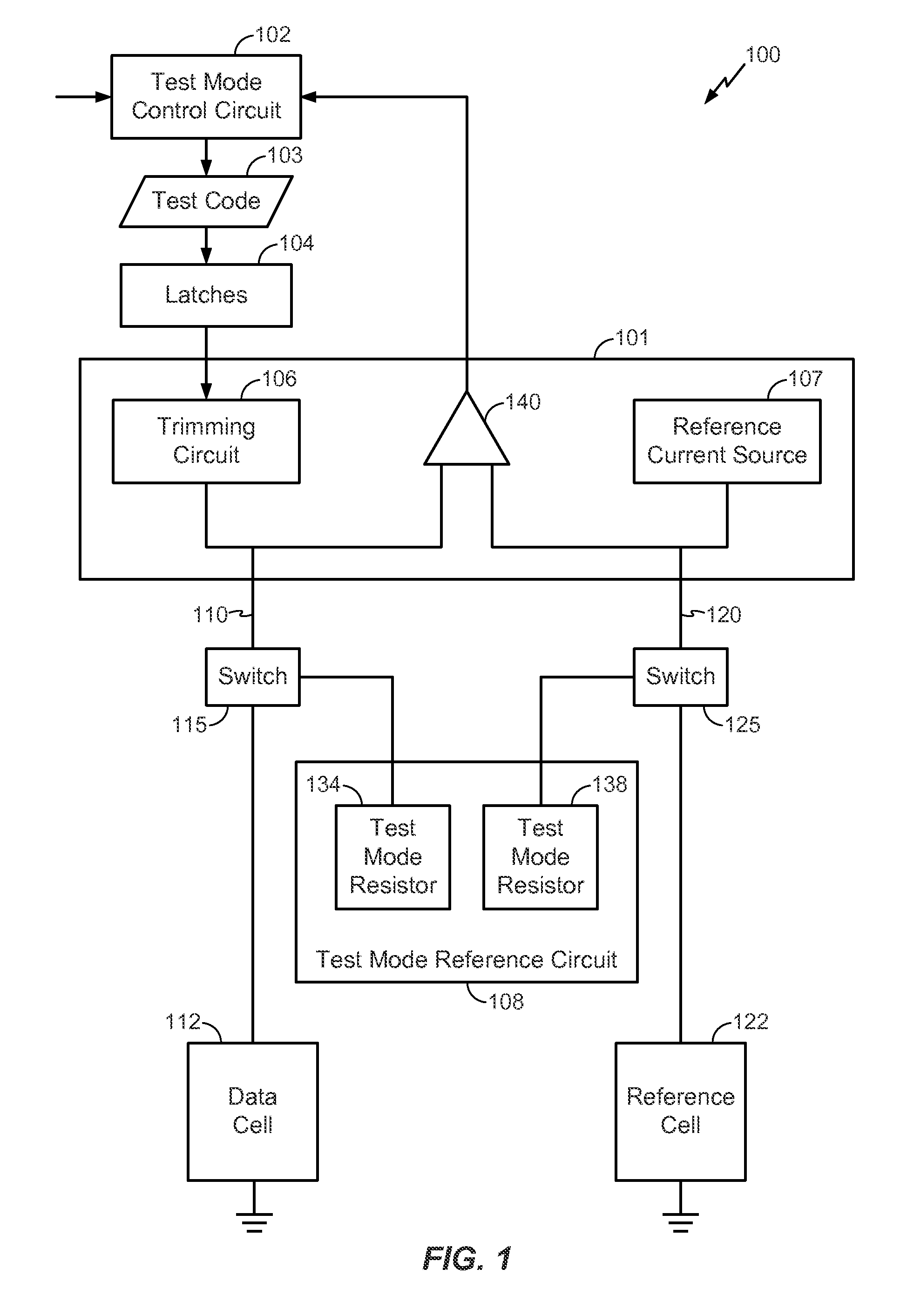
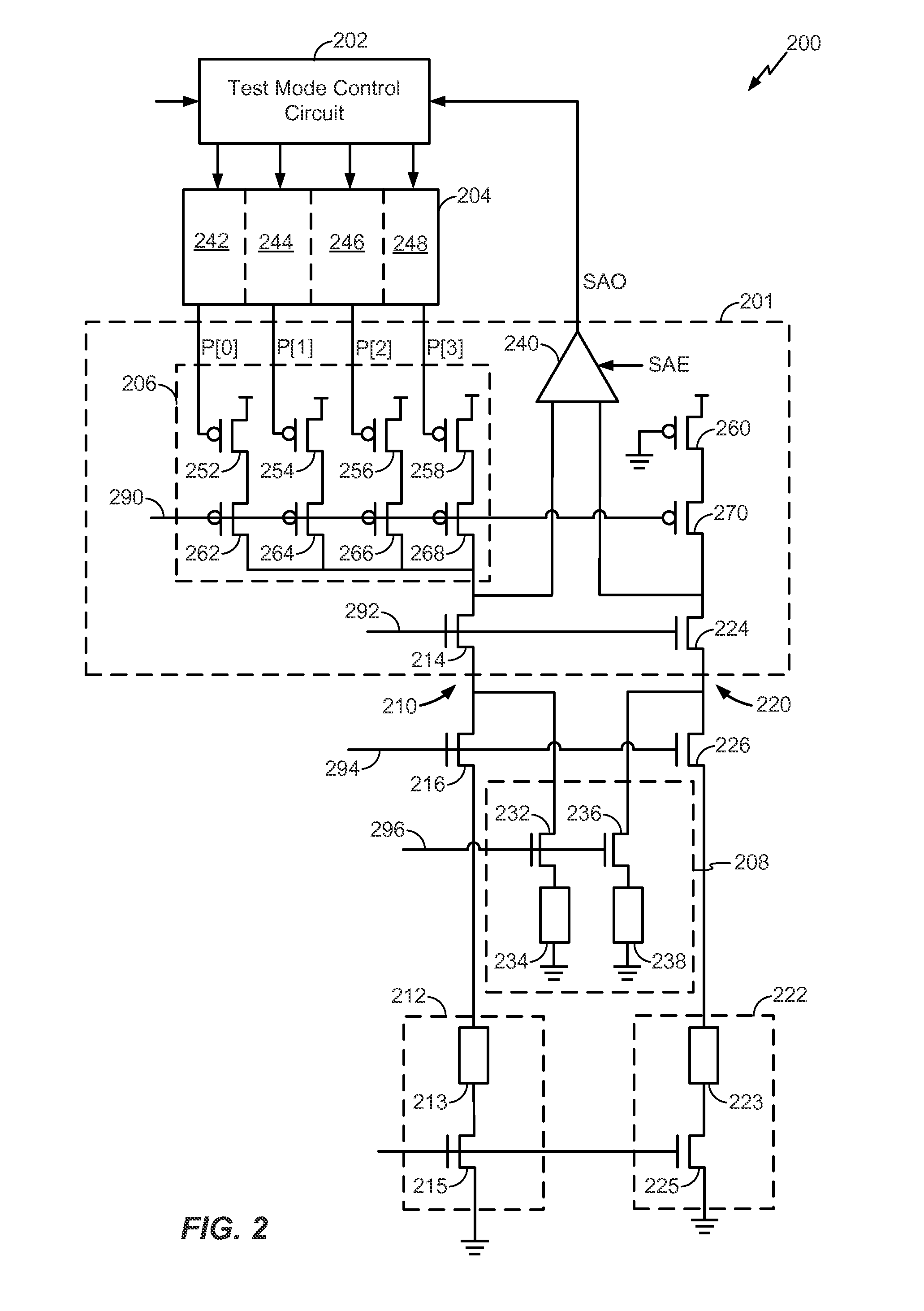
[0018]Referring to FIG. 1, a particular illustrative embodiment of a memory system 100 that is operable to reduce or cancel a voltage offset during sensing operations is shown. The memory system 100 includes a sense amplifier 101, a test mode control circuit 102, a plurality of latches 104, a test mode reference circuit 108, a data cell 112, and a reference cell 122. The sense amplifier 101 includes a trimming circuit 106, a reference current source 107, and a comparator 140.

[0019]The data cell 112 may be a memory cell within a magnetoresistive random access-memory (MRAM), a phase change random access memory (PRAM), a spin-transfer torque magnetoresistive random-access memory (STT-MRAM), a ferroelectric random-access memory (FRAM), or a resistive random-access memory (ReRAM), as illustrative, non-limiting examples. For example, the data cell 112 may be a memory cell within a non-volatile memory. The data cell 112 includes a programmable resistance based memory element. In a particul...


PUM


Abstract

A circuit includes a plurality of transistors responsive to a plurality of latches that store a test code. The circuit further includes a first bit line coupled to a data cell and coupled to a sense amplifier. The circuit also includes a second bit line coupled to a reference cell and coupled to the sense amplifier. A current from a set of the plurality of transistors is applied to the data cell via the first bit line. The set of the plurality of transistors is determined based on the test code. The circuit also includes a test mode reference circuit coupled to the first bit line and to the second bit line.

Description

I. FIELD[0001]The present disclosure is generally related to characterization of and compensation for sense amplifier voltage offset.II. DESCRIPTION OF RELATED ART[0002]Advances in technology have resulted in smaller and more powerful computing devices. For example, there currently exist a variety of portable personal computing devices, including wireless computing devices, such as portable wireless telephones, personal digital assistants (PDAs), and paging devices that are small, lightweight, and easily carried by users. More specifically, portable wireless telephones, such as cellular telephones and internet protocol (IP) telephones, can communicate voice and data packets over wireless networks. Further, many such wireless telephones include other types of devices that are incorporated therein. For example, a wireless telephone can also include a digital still camera, a digital video camera, a digital recorder, and an audio file player. Also, such wireless telephones can process e...

Claims


Application Information

Patent Timeline
Patent Type & Authority Patents(United States)
IPC IPC(8): G11C7/00G11C16/28G11C29/02G11C29/46G11C29/44G11C29/14G01R31/28
CPCG11C29/02G11C29/026G11C29/028G11C29/14G11C29/44G11C29/46G01R31/2851G11C16/28
Inventor KIM, JUNG PILLKIM, TAEHYUNKIM, SUNGRYULKIM, DAEIK D.
Owner QUALCOMM INC
Why Eureka
Try Eureka