Multi-phase models for timing closure of integrated circuit designs

a technology of integrated circuits and timing analysis, applied in the direction of instruments, computing, electric digital data processing, etc., can solve the problems of time-consuming and laborious timing analysis, difficult to share the computational load of flattened chip level netlists with other networked computers, and difficult to perform timing analysis of an integrated circuit chip. achieve the effect of accurate modeling

Active Publication Date: 2015-10-06
CADENCE DESIGN SYST INC
View PDF33 Cites 5 Cited by
  • Summary
  • Abstract
  • Description
  • Claims
  • Application Information

AI Technical Summary

Problems solved by technology

However, timing closure by an EDA tool may be more difficult to obtain with a flattened chip level netlist on an entire integrated circuit.
Additionally, one computer system is typically used to perform a timing analysis on a flattened chip level netlist, as it is difficult to share the computational load of a flattened chip level netlist with other networked computers.
With a limited amount of computer resources, the time to perform a timing analysis of an entire integrated circuit chip may be quite long given today's complicated integrated circuits.
As mentioned herein, each clock entry path may have multiple clock paths resulting in multiple clock timing delay values for the respective clock entry point.
However, neither timing arc 502 nor timing arc 503 considers that there may be an inter partition delay in the clock path.
If a timing budget is not being met along a data signal path or a clock signal path, the path may be flagged as failing.
Previously, the design flow process to achieve signal timing goals was repetitive (not single pass) and difficult to partition into parallel independent jobs.
Without accurate clock network delays, the data timing budgets generated for partitions could be poor, such that timing closure may not be achieved.
Without clock latency modeling, the library models generated by data time budgeting are mostly useless during clock tree synthesis at the top level.
Previously, the timing budgeting process did not efficiently process the condition where both a single cycle path (SCP) and a multi-cycle path (MCP) coexisted.
Discarding the timing information for either the single cycle path (SCP) or the multi-cycle path (MCP) may result in circuits not being analyzed accurately by the time budgeting process.
Inaccurate timing may lead to the integrated circuit (IC) design being non-implementable and require manual edits by the designer in order to resolve the timing problem(s).
The multi-cycle path (MCP) 1224 with more stringent constraints may not be implementable resulting in an inoperable integrated circuit design.
The single cycle path (SCP) may then have overly pessimistic timing constraints and may not be implementable.
Without the timing information for the single cycle path (SCP), the timing of the top level determined during the time budgeting process may be inaccurate.
Without the embodiments of the invention, two of the four paths timing delay information would not be evaluated by the time budgeting process and hence a potential decrease in timing accuracy.
This may lead to an increase of time-costly hand edits and or potentially, integrated circuits that may not be implementable.
However, without the embodiments of the invention, exceptions such as multi-cycle paths (MCP) and max delay paths (MDP) are not accurately modeled for timing delays and the time budget goals may not be achieved.

Method used


Image

  • Multi-phase models for timing closure of integrated circuit designs
  • Multi-phase models for timing closure of integrated circuit designs
  • Multi-phase models for timing closure of integrated circuit designs

Examples


Embodiment Construction

[0040]In the following detailed description of the embodiments of the invention, numerous specific details are set forth in order to provide a thorough understanding of the aspects of the invention. However, it will be obvious to one skilled in the art that the embodiments of the invention may be practiced without these specific details. In other instances well known methods, procedures, components, and circuits have not been described in detail so as not to unnecessarily obscure aspects of the invention.

[0041]Reference in the specification to “one embodiment” or “an embodiment” means that a particular feature, structure, or characteristic described in connection with the embodiment is included in at least one embodiment of the invention. The appearances of the phrase “in one embodiment” in various places in the specification do not necessarily all refer to the same embodiment.

INTRODUCTION

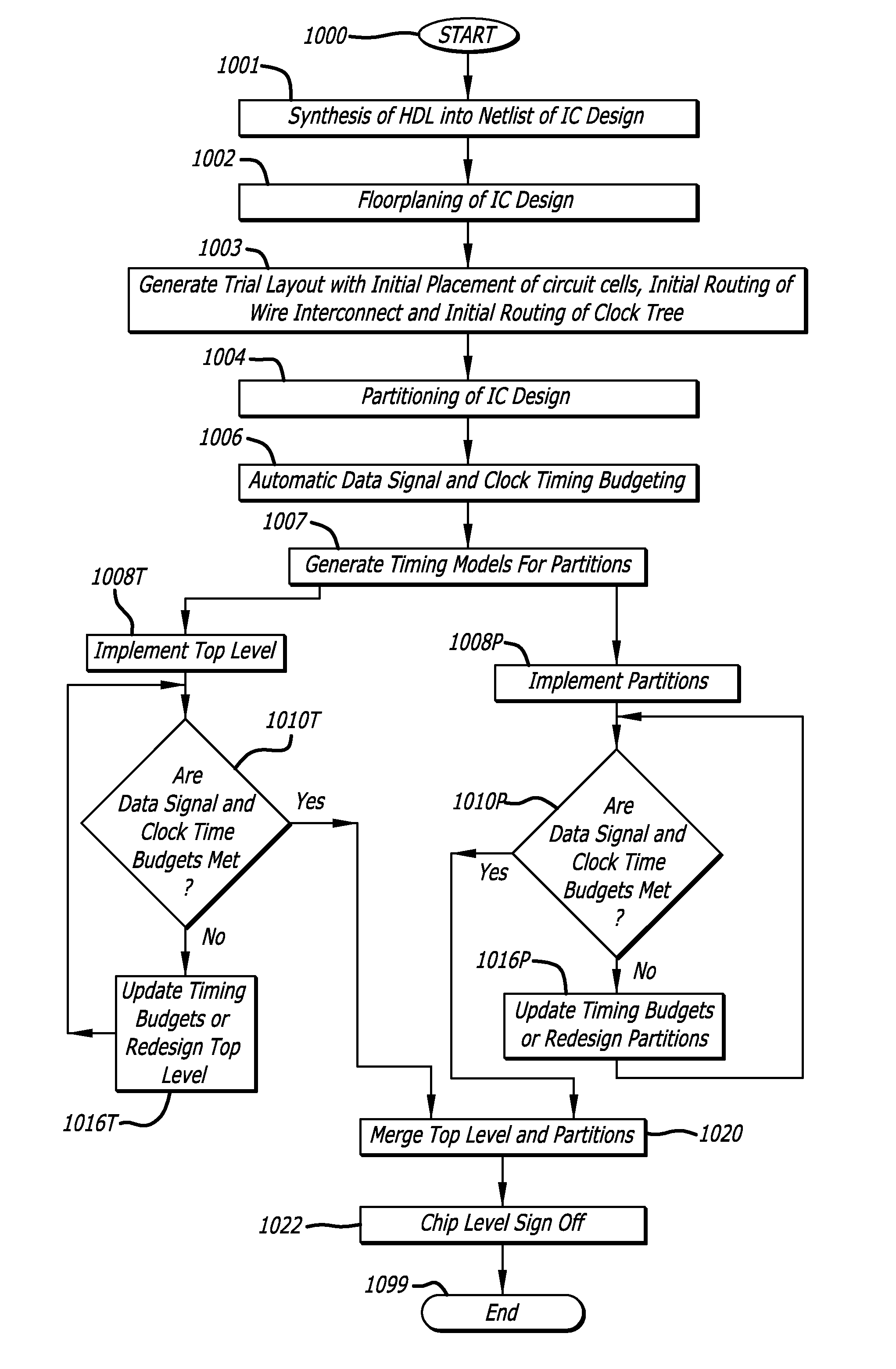
[0042]The embodiments of the invention facilitate budgeting of clock signal timing between func...


PUM


Abstract

In one embodiment, a method of designing an integrated circuit is disclosed, including receiving a first partition block for a top level of a hierarchical design of an integrated circuit; analyzing each pin of the first partition block for an attribute associated with the pin indicating a timing exception; and if a timing exception other than false path is indicated then generating an internal timing pin in a first timing graph model of the first partition block for each timing exception, and adding a timing arc and a dummy arc coupled to the internal timing pin in the first timing graph model of the first partition block. The internal timing pin adds a timing exception constraint for each timing exception. Timing of the top level may then be analyzed with the first timing graph model to determine if timing constraints, including the added timing exception constraints, are met.

Description

CROSS-REFERENCE TO RELATED APPLICATIONS[0001]The present application is a divisional of and claims the benefit of U.S. patent application Ser. No. 12 / 897,777, entitled MULTI-PHASE MODELS FOR TIMING CLOSURE OF INTEGRATED CIRCUIT DESIGNS, filed on Oct. 4, 2010 by Dinesh Gupta et al., now allowed. U.S. patent application Ser. No. 12 / 897,777 is a continuation in part and claims the benefit of U.S. Pat. No. 8,365,113 entitled FLOW METHODOLOGY FOR SINGLE PASS PARALLEL HIERARCHICAL TIMING CLOSURE OF INTEGRATED CIRCUIT DESIGNS filed on Feb. 18, 2010 by inventors Vivek Bhardwaj et al. which in turn claims the benefit of U.S. Provisional Patent Application No. 61 / 265,705 entitled FLOW METHODOLOGY FOR SINGLE PASS PARALLEL HIERARCHICAL TIMING CLOSURE OF INTEGRATED CIRCUIT DESIGNS filed on Dec. 1, 2009 by inventors Vivek Bhardwaj et al.; and which is a continuation in part and claims the benefit of U.S. Pat. No. 8,504,978 entitled USER INTERFACE FOR TIMING BUDGET ANALYSIS OF INTEGRATE CIRCUIT DE...

Claims


Application Information

Patent Timeline
Patent Type & Authority Patents(United States)
IPC IPC(8): G06F9/455G06F17/50
CPCG06F17/50G06F30/327G06F2119/12G06F30/00G06F30/3315
Inventor GUPTA, DINESHLEVITSKY, OLEG
Owner CADENCE DESIGN SYST INC
Why Eureka
Try Eureka