Calibrating a wire load model for an integrated circuit

a wire load model and integrated circuit technology, applied in the field of calibration of wire load models for integrated circuits, can solve the problems of increasing the difficulty of characterizing, increasing the criticality of the wire load model, and increasing the time and money required to design, fabricate and test such integrated circuits

Inactive Publication Date: 2006-12-12
RENESAS ELECTRONICS AMERICA
View PDF33 Cites 12 Cited by
  • Summary
  • Abstract
  • Description
  • Claims
  • Application Information

AI Technical Summary

Problems solved by technology

A substantial amount of time and money is needed to design, fabricate, and test such integrated circuits.
This process can be expensive and time consuming.
As the minimum feature sizes of integrated circuits continue to shrink and operating speeds increase, the effects on signal delay due to the resistive, capacitive, and inductive parasitics of nets (e.g., wiring) which interconnect the active devices of the integrated circuit become more critical and more difficult to characterize.
However, as the minimum feature sizes of integrated circuits continue to shrink, the ratio of interconnect net delay to total delay has increased substantially.
Estimating the parasitics for each wire is one of the problems which arise during attempts to achieve timing closure in the design of an integrated circuit.
As such, the actual parasitic effects on signal delay cannot be accurately predicted at the front end of the design phase.
But even if the estimated lumped RLC at the front end matches total RLC at the back end, the timing would not match, since the effect of distribution of the lumped RLC is neglected in the front end.
Another problem is the lack of one-to-one correspondence of logical and physical wires.
Timing exceptions (i.e. exclusion of non-relevant paths from analysis) may be handled differently by different engines, or the user may have made mistakes in specifying the intentionally equivalent timing exceptions in different tool-specific languages.
This problem would be solved by using the same timing engine for each design step, but this is often not possible.
In some instances, even with a large number of iterations, the timing correlation cannot be satisfied.
Under design leads to excessive iterations, increasing the cost and delaying the production of the design.
In the case of over design, the lack of timing correlation leads to a circuit which is larger, slower or consumes more power than necessary to accomplish the desired function.

Method used


Image

  • Calibrating a wire load model for an integrated circuit
  • Calibrating a wire load model for an integrated circuit
  • Calibrating a wire load model for an integrated circuit

Examples


Embodiment Construction

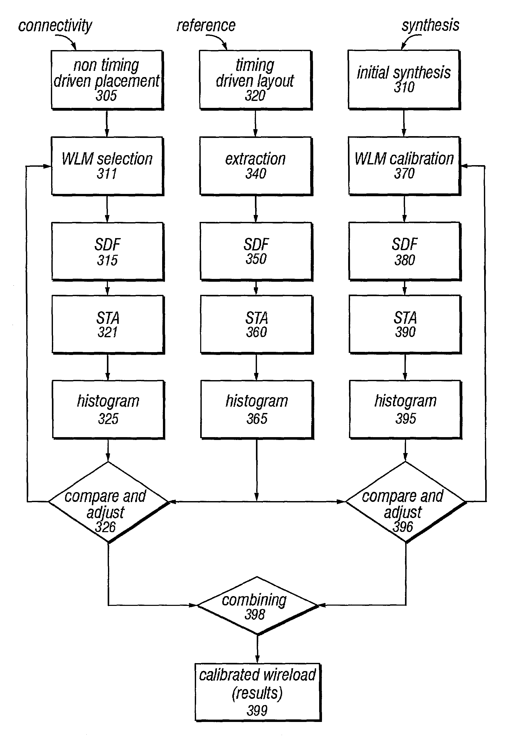
[0032]The following sets forth a detailed description of a mode for carrying out the invention. The description is intended to be illustrative of the invention and should not be taken to be limiting. As previously described, accurate timing management throughout the design process is necessary for an integrated circuit to operate correctly. The length of net connections in an integrated circuit determines the operating frequency, or speed, of the chip. The objective is a design with the shortest possible connections. Similarly, an integrated circuit with shorter net connections will be a smaller chip. A method to select the shortest possible connections will result in a design with the optimum solution for area and timing. The desired solution for area and timing produces a minimum of timing slacks with no timing violations.

[0033]The present invention provides timing correlation before and after layout and balances timing margins. Balancing the timing margin of an integrated circuit...


PUM


Abstract

A method is taught for determining a calibrated wire load model. The calibrated wire load model can be used to reach timing closure for an integrated circuit. The method includes; determining a reference timing description; determining a wire load model based on synthesis; determining a wire load model based connectivity; comparing the wire load model based on connectivity to the reference timing description. The method teaches adjusting the wire load model based on connectivity to determine a wire load model which faciliates timing closure. The method also teaches comparing the wire load model (based on synthesis) with the reference timing description. The disclosure contemplates a computer program product based upon the method taught. The disclosure further contemplates an integrated circuit designed based on the method taught. In another embodiment a computer system or another electronic system includes an integrated circuit designed by the method taught.

Description

CROSS-REFERENCE TO RELATED APPLICATION[0001]This application relates to co-pending U.S. patent application Ser. No. 09 / 946,240, filed on Sep. 5, 2001, entitled “Timing Optimization and Timing Closure for Integrated Circuit Models” naming Wolfgang Roethig and Attila Kovacs-Birkas as inventors, which is assigned to the assignee of this application, the application being hereby incorporated herein by reference in its entirety.[0002]This application relates to co-pending U.S. patent application Ser. No. 09 / 878,497, filed on Jun. 11, 2001, entitled “Cell Modeling In the Design of An Integrated Circuit” naming Attila Kovacs-Birkas as inventor, which is assigned to the assignee of this application, the application being hereby incorporated herein by reference in its entirety.BACKGROUND OF THE INVENTION [0003]Present day ultra-large-scale integration (ULSI) circuits may include millions of interconnected active electronic devices fabricated on a silicon substrate and operating at clock rate...

Claims


Application Information

Patent Timeline
Patent Type & Authority Patents(United States)
IPC IPC(8): G06F17/50
CPCG06F17/5031G06F17/5036G06F30/3312G06F30/367
Inventor KOVACS-BIRKAS, ATTILAROETHIG, WOLFGANGHADDAD, NADER J.
Owner RENESAS ELECTRONICS AMERICA
Why Eureka
Try Eureka