Achieving Clock Timing Closure in Designing an Integrated Circuit

a technology of clock timing and integrated circuit, which is applied in the direction of computer aided design, program control, instruments, etc., can solve the problems of clock timing violations, clock may be so restricted, and signals that do not properly synchronize the data path components are said to have clock timing violations, etc., to achieve the effect of enhancing overall design convergen

Active Publication Date: 2010-03-18
CADENCE DESIGN SYST INC
View PDF17 Cites 13 Cited by
  • Summary
  • Abstract
  • Description
  • Claims
  • Application Information

AI Technical Summary

Benefits of technology

[0007]Overall design convergence is enhanced by a process that emulates CTS at a point in the design process after the initial placement is made of “high-level” primary clock path components and before the actual CTS stage instantiates the clock network. As a result, clock delays can be virtually determined and propagated through the initial clock network to further virtually determine the clock gating setup violations.

Problems solved by technology

Those clock signals that do not properly synchronize the data path components are said to have clock timing violations, including clock gating setup violations.
True clock timing violations can be seen during the design process only after the CTS stage, once the clock timing is in propagated clock mode.
However, it is often too late during the design process to fix the clock gating setup violations after the CTS stage, because there has typically been a lot of data path optimization that happened before the CTS stage that may have greatly restricted the options for further modifications.
Additionally, the clock may be so restricted that the data path optimizers may not fulfill the requirements for data path signal arrival times. Although the pre-CTS optimizers operate on the clock gating setup violations, the pre-CTS optimizers may not even “see” the clock delays and clock gating setup violations, since the clock is in ideal clock mode during that part of the design process.
Additi

Method used


Image

  • Achieving Clock Timing Closure in Designing an Integrated Circuit
  • Achieving Clock Timing Closure in Designing an Integrated Circuit
  • Achieving Clock Timing Closure in Designing an Integrated Circuit

Examples


Embodiment Construction

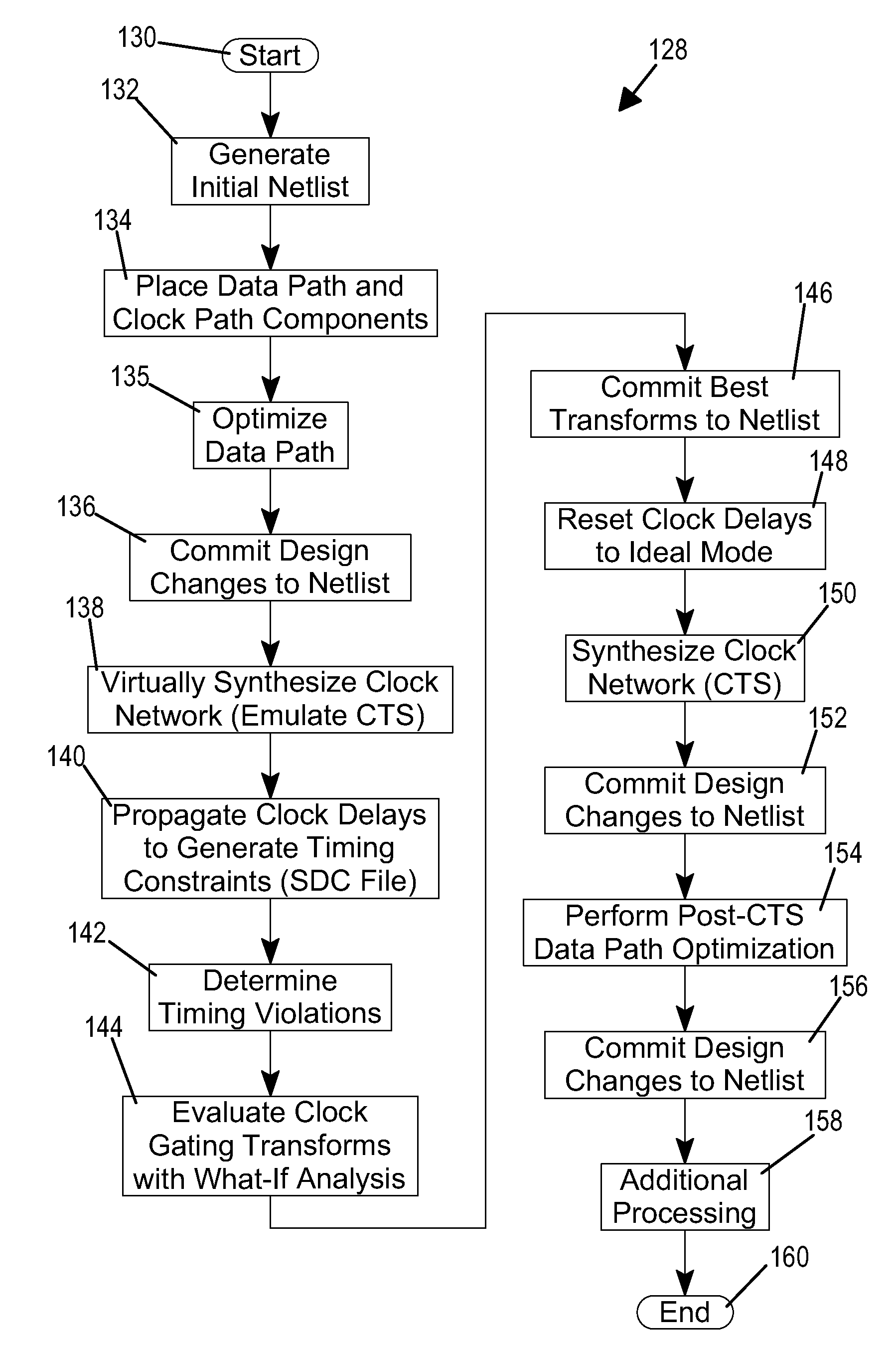
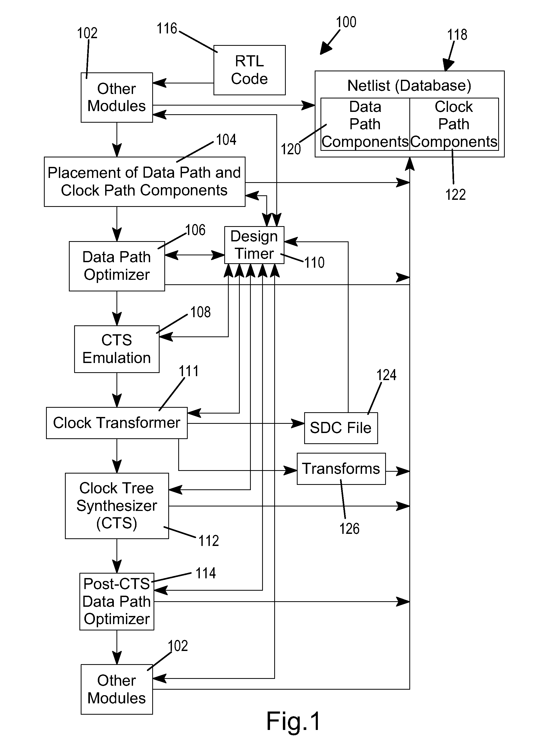
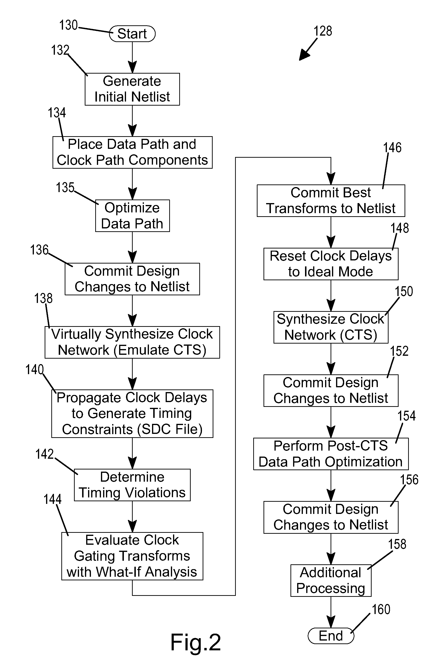
[0011]Tools for designing an integrated circuit typically include several modules (representing design “stages”) that perform various functions of the design process. Schematic diagram 100, FIG. 1, shows an exemplary set of such modules 102-114 (used in a simplified flow of a design process similar to that available in the “Cadence Encounter Digital IC Design Platform”) that includes additional modules, features or functions (described below) that enable more rapid and efficient fixing of clock timing violations, such as clock gating setup violations, and more rapid and efficient overall design convergence than is available in the prior art. These advantages are primarily achieved by a design process that emulates clock tree synthesis (CTS) at an earlier point in the design flow than the point at which actual CTS is performed to instantiate the clock circuitry. In other words, the clock tree, or clock network, is virtually synthesized, so it becomes possible to calculate clock delay...


PUM


Abstract

Achieving clock timing closure in designing an integrated circuit involves virtually synthesizing a clock network for the integrated circuit design to generate virtual clock buffering in the clock network before a point in the design flow at which the clock network is actually synthesized and committed to a netlist. Timing violations are determined for clock gates generated by the virtual clock buffering. Clock gating transforms are evaluated for the clock gates having the timing violations, based on recalculated clock and data path delays, to incrementally virtually synthesize the clock network. The clock gating transforms that result in the best timing gains are committed to the netlist. The clock network is then actually synthesized for the integrated circuit design, and design changes, due to the actual clock network synthesis, are committed to the netlist.

Description

BACKGROUND OF THE INVENTION[0001]In the design process for an integrated circuit, an initial “high-level” description of the circuitry must be converted into a description of an actual physical implementation of the circuitry in silicon. The description of the physical implementation generally includes all of the electronic components (i.e. transistors, diodes, resistors, capacitors, inductors, adders, multipliers, flip-flops, gates, buffers, etc.) and the paths (i.e. electrical conductor traces) for all of the signals between all of the components. Some of these signal paths are for the data that produce the overall function of the integrated circuit. Additionally, some of the signal paths are for one or more clock signals that trigger the function of some of the electronic components, such as flip-flops.[0002]Some of the electronic components must be synchronized with others of the electronic components in order to ensure that these electronic components receive the correct data s...

Claims


Application Information

Patent Timeline
IPC IPC(8): G06F17/50
CPCG06F17/505G06F2217/84G06F2217/62G06F30/327G06F30/396G06F2119/12G06F2117/04
Inventor SIRCAR, SOURAV KUMARBARONIA, MANISH
Owner CADENCE DESIGN SYST INC
Why Eureka
Try Eureka