Method of patterning a low-k dielectric film

a dielectric film and low-k technology, applied in the field of semiconductor processing, can solve problems such as adversely affecting the performance of devices

Active Publication Date: 2015-10-20
APPLIED MATERIALS INC
View PDF19 Cites 113 Cited by
  • Summary
  • Abstract
  • Description
  • Claims
  • Application Information

AI Technical Summary

Problems solved by technology

As components have scaled and transistors have moved closer together, the insulating dielectrics have thinned to the point where charge build-up and crosstalk adversely affect the performance of the device.

Method used


Image

  • Method of patterning a low-k dielectric film
  • Method of patterning a low-k dielectric film
  • Method of patterning a low-k dielectric film

Examples


Embodiment Construction

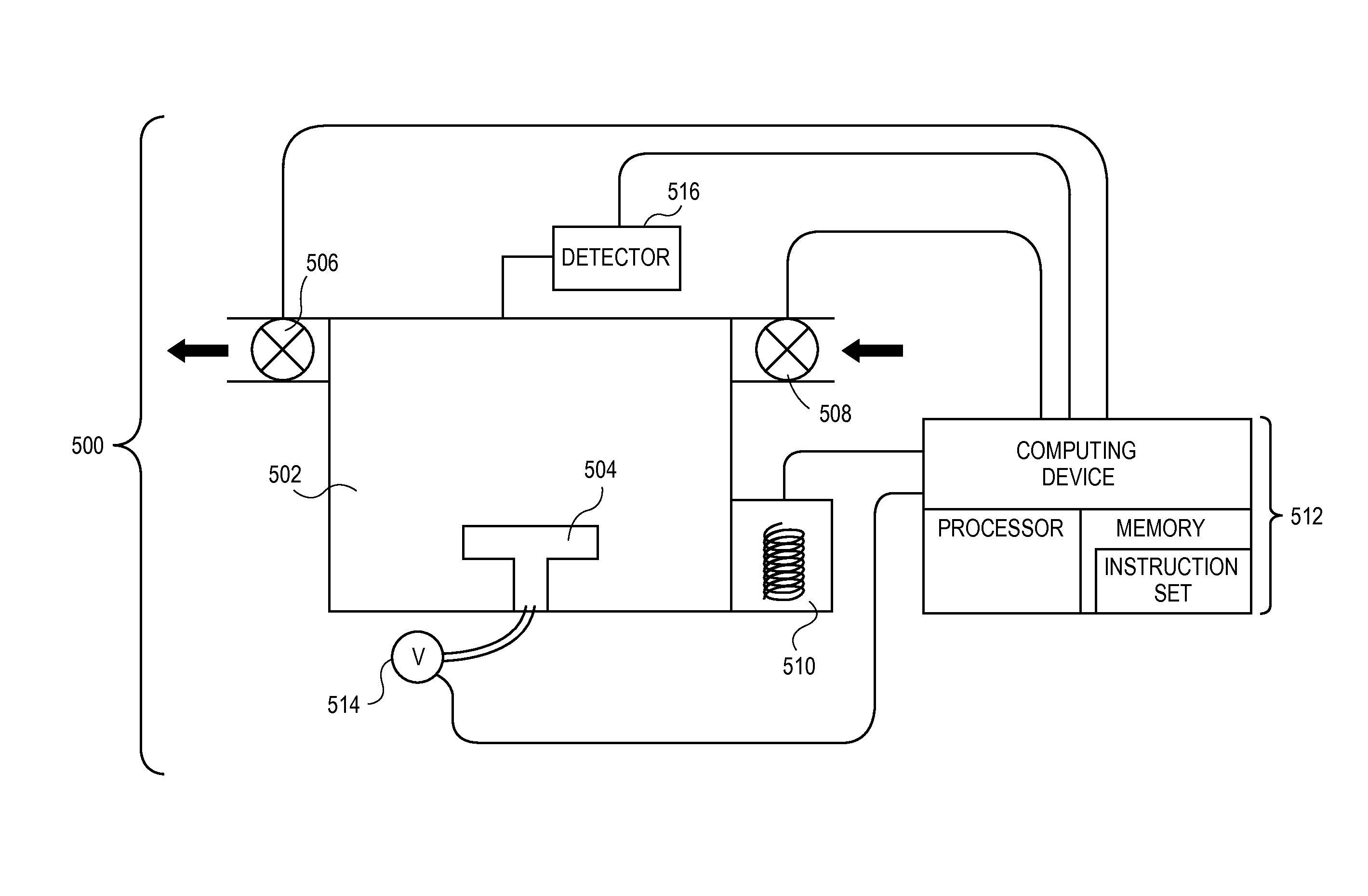
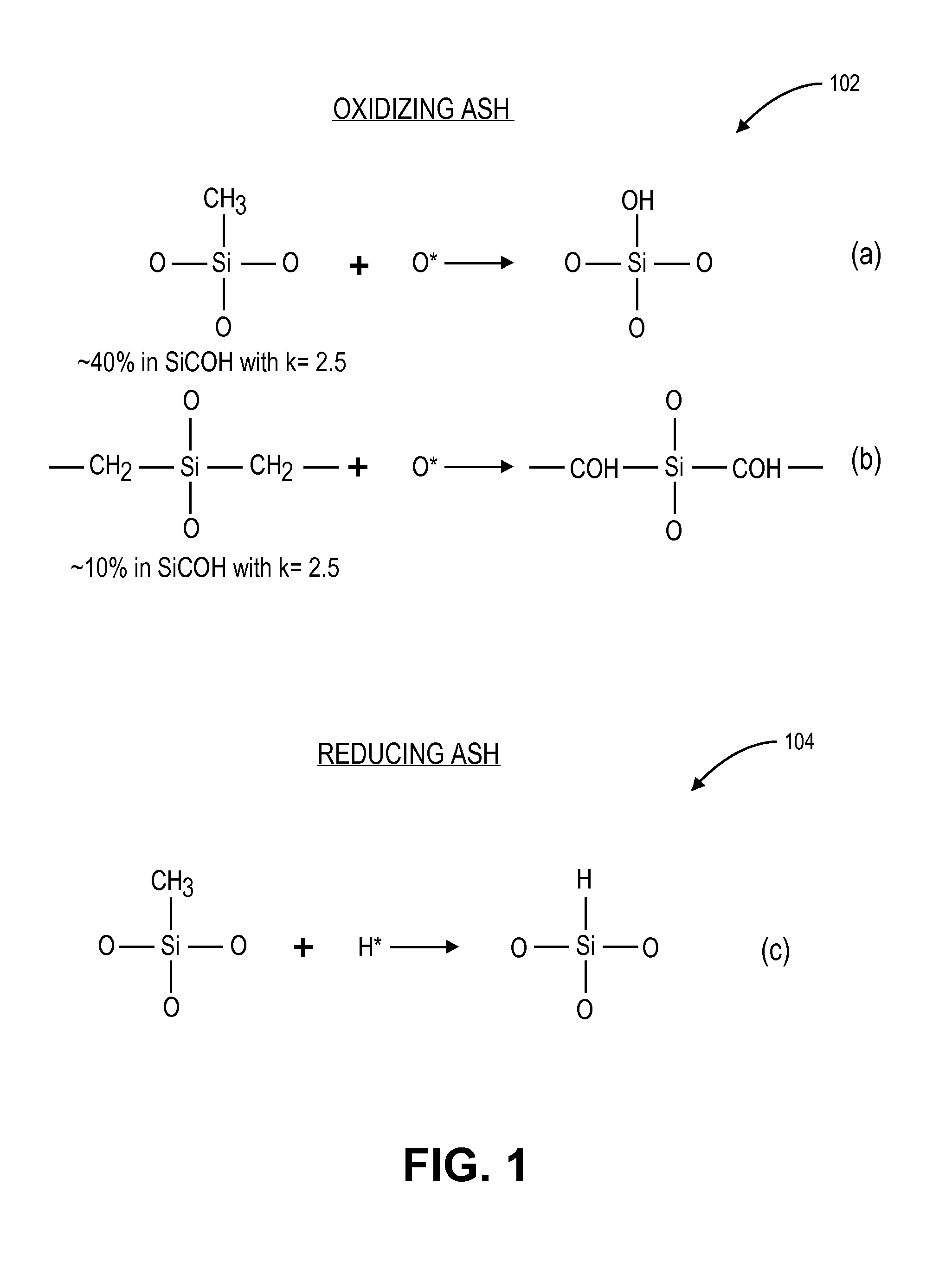
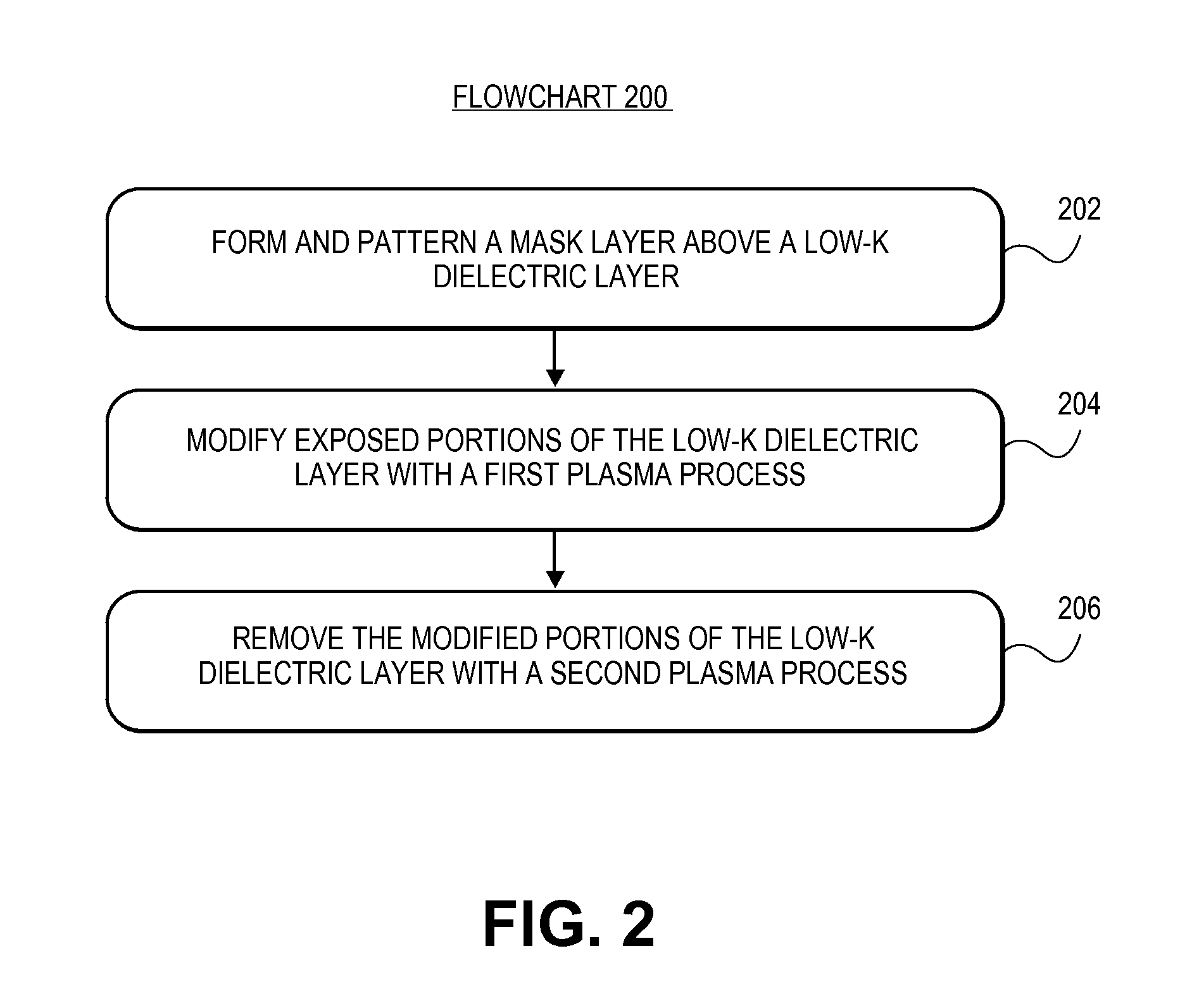
[0019]Methods of patterning low-k dielectric films are described. In the following description, numerous specific details are set forth, such as specific plasma treatments and effects for modifying portions of low-k dielectric films, in order to provide a thorough understanding of embodiments of the present invention. It will be apparent to one skilled in the art that embodiments of the present invention may be practiced without these specific details. In other instances, well-known aspects, such as photolithography patterning and development techniques for mask formation, are not described in detail in order to not unnecessarily obscure embodiments of the present invention. Furthermore, it is to be understood that the various embodiments shown in the Figures are illustrative representations and are not necessarily drawn to scale.

[0020]New approaches and processing sequences for etching low k films damage-free to the low k are described. Traditional dielectric etching is can result ...


PUM


Abstract

Methods of patterning low-k dielectric films are described. In an example, a method of patterning a low-k dielectric film involves forming and patterning a mask layer above a low-k dielectric layer, the low-k dielectric layer disposed above a substrate. The method also involves modifying exposed portions of the low-k dielectric layer with a nitrogen-free plasma process. The method also involves removing, with a remote plasma process, the modified portions of the low-k dielectric layer selective to the mask layer and unmodified portions of the low-k dielectric layer.

Description

CROSS-REFERENCE TO RELATED APPLICATIONS[0001]This application claims the benefit of U.S. Provisional Application No. 61 / 721,414, filed on Nov. 1, 2012, the entire contents of which are hereby incorporated by reference herein.BACKGROUND[0002]1) Field[0003]Embodiments of the present invention pertain to the field of semiconductor processing and, in particular, to methods of patterning low-k dielectric films.[0004]2) Description of Related Art[0005]In semiconductor manufacturing, a low-k dielectric is a material with a small dielectric constant relative to silicon dioxide. Low-k dielectric material implementation is one of several strategies used to allow continued scaling of microelectronic devices. In digital circuits, insulating dielectrics separate the conducting parts (e.g., wire interconnects and transistors) from one another. As components have scaled and transistors have moved closer together, the insulating dielectrics have thinned to the point where charge build-up and crosst...

Claims


Application Information

Patent Timeline
Patent Type & Authority Patents(United States)
IPC IPC(8): H01L21/302H01L21/3105H01L21/311H01L21/02
CPCH01L21/3105H01L21/31116H01L21/31138H01L21/02126H01J37/32009H01J37/3244
Inventor NEMANI, SRINIVAS D.PENDER, JEREMIAH T.ZHOU, QINGJUNLUBOMIRSKY, DMITRYBELOSTOTSKIY, SERGEY G.
Owner APPLIED MATERIALS INC
Why Eureka
Try Eureka