
Eureka
For R&D, Eureka makes reading and utilizing patents & technical documents easy.
Eureka AIR
Designed for self-driven R&D workflows. Generate viable solutions, solve complex R&D challenges, empower your innovation with AI.

Eureka Materials
Designed for material experts only. Revolutionize your material R&D, from search, analyze, to developing new materials.

TechResearch
Generate reliable direction feasibility study reports for your R&D in just a few steps.

TechSeek
Discover and master advanced knowledge NOW. Basics, ideas, possibilities, all at once.

TechMind
As an expert in R&D Theories, TechMind can generates customized viable solutions instantly.

TechRisk
Analyze your overall solution with one click, know your potential R&D risks in advance.

TechMonitor
Get weekly tech updates, stay abreast of the latest tech innovations and key insights.
Partial glob-top encapsulation technique
- Summary
- Abstract
- Description
- Claims
- Application Information
AI Technical Summary
Benefits of technology
Problems solved by technology
Method used
Image

Examples
Embodiment Construction
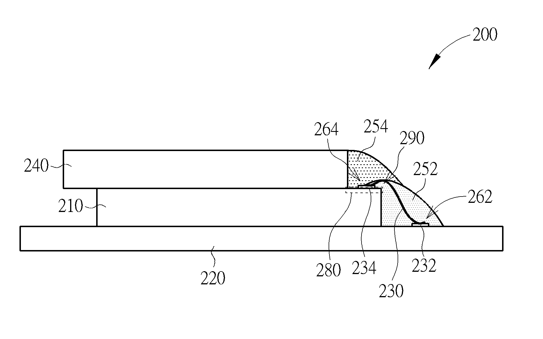
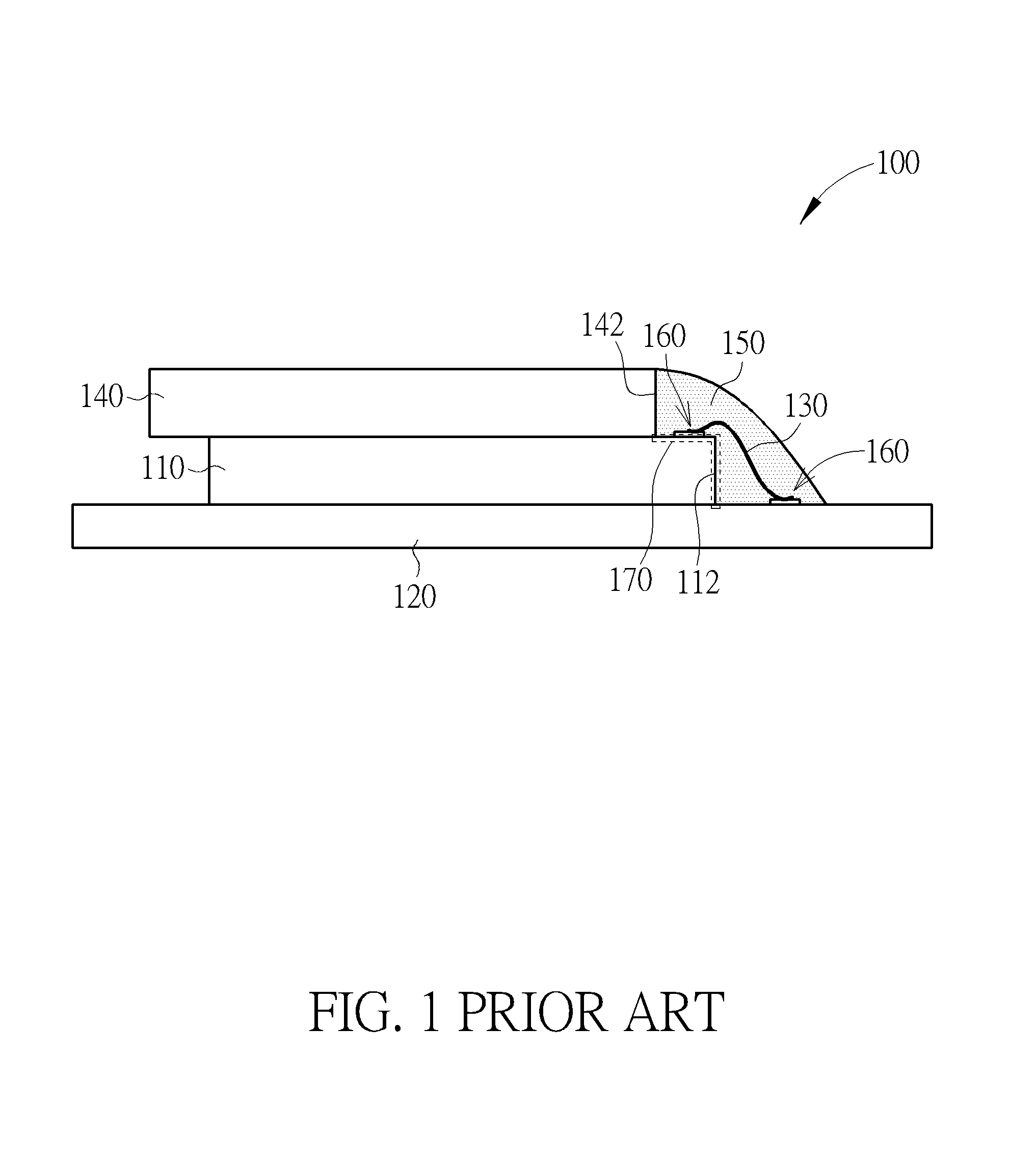
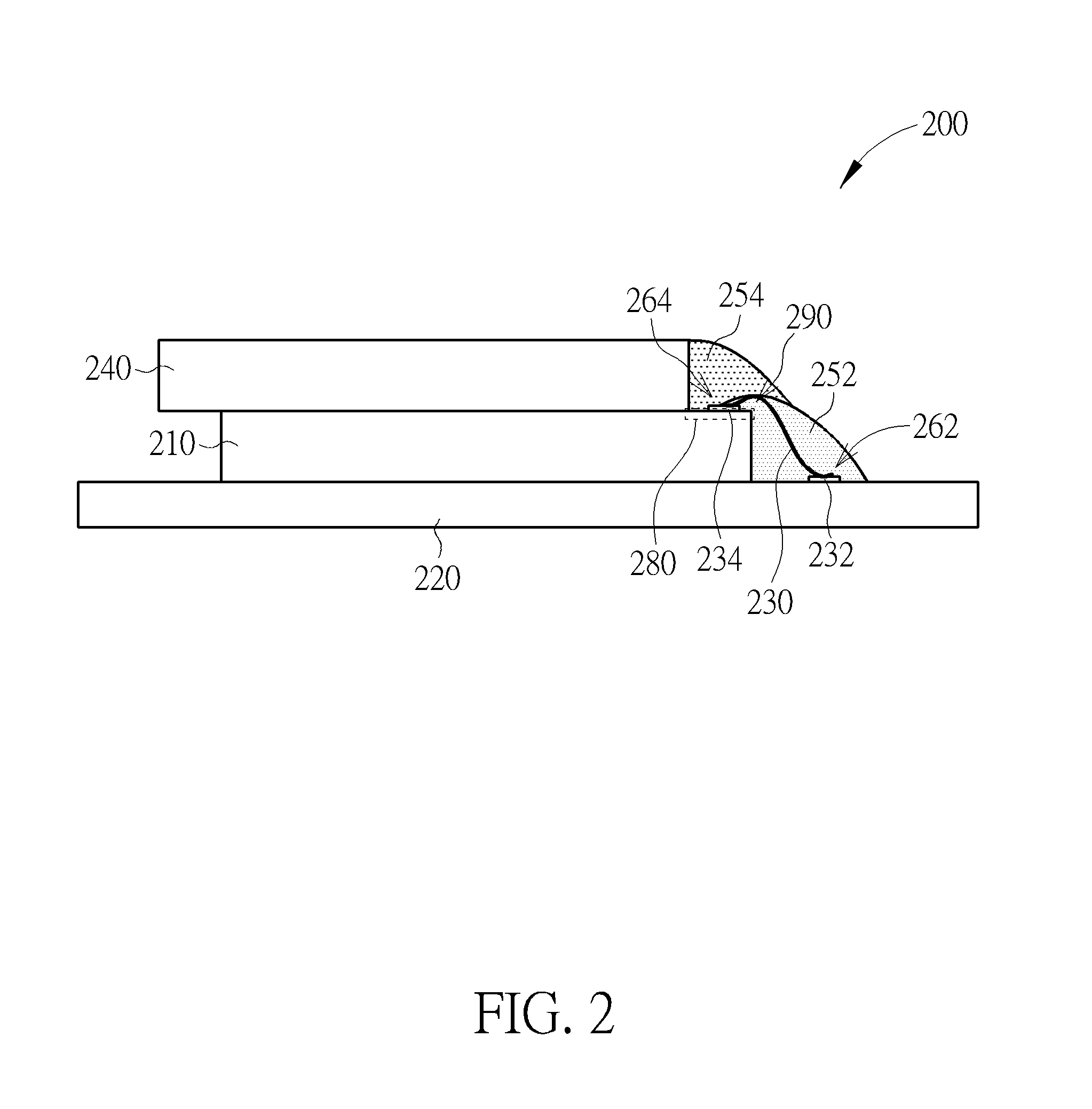
[0016]Please refer to FIG. 2, which illustrates an electronic device 200 according to one exemplary embodiment of the present invention. As shown by figure, a semiconductor device 210 is attached to a circuit board 220. In various embodiments, the circuit board 220 could be a printed circuit board or a flexible printed circuit. The semiconductor device 210 could be a bare die or a silicon backplane of an LCoS device, while the electronic device 200 could be an LCoS device or a COB assembly. A cover material 240 is disposed above the semiconductor device 210, which could be a cover glass.
[0017]There are a plurality of metal bonding wires (e.g. aluminum wires) 230 connected between the semiconductor device 210 and a circuit board 220. A plurality of first bonds 264 are formed by electrically connecting (e.g. soldering) first ends of the bonding wires 230 respectively to a plurality of contact pads 234 on the semiconductor device 210, and a plurality of second bonds 262 are formed by e...
PUM
 Abstract
Description
Claims
Application Information
 - R&D Engineer
- R&D Manager
- IP Professional
- Industry Leading Data Capabilities
- Powerful AI technology
- Patent DNA Extraction
Browse by: Latest US Patents, China's latest patents, Technical Efficacy Thesaurus, Application Domain, Technology Topic, Popular Technical Reports.
© 2024 PatSnap. All rights reserved.Legal|Privacy policy|Modern Slavery Act Transparency Statement|Sitemap|About US| Contact US: help@patsnap.com