Integrating multi-output power converters having vertically stacked semiconductor chips

a technology of vertical stacking and power converter, which is applied in the direction of semiconductor devices, semiconductor/solid-state device details, electrical apparatus, etc., can solve the problems of significant parasitic impedance into the power circuit, and achieve the effect of avoiding parasitic impedances

Active Publication Date: 2015-12-15
TEXAS INSTR INC
View PDF18 Cites 27 Cited by
  • Summary
  • Abstract
  • Description
  • Claims
  • Application Information

AI Technical Summary

Benefits of technology

[0012]As a result of the integration, the device with multi-output power switches avoids altogether the parasitic impedances of PCB traces. In addition, the stacked power FETs offer thermal and electrical efficiencies close to the theoretical maximum. The device permits direct implementation into PCBs without the headache of first modifying a footprint.

Problems solved by technology

The electrical connections from the chips to the leads may be provided by bonding wires, which introduce, due to their lengths and resistances, significant parasitic inductance into the power circuit.
Independent of the physical size, the sync FET chip needs a larger active area than the active area of the control FET chip, due to considerations of duty cycle and conduction loss.

Method used


Image

  • Integrating multi-output power converters having vertically stacked semiconductor chips
  • Integrating multi-output power converters having vertically stacked semiconductor chips
  • Integrating multi-output power converters having vertically stacked semiconductor chips

Examples


Embodiment Construction

[0026]Embodiments of a single electronic device creating two or more outputs from a single input can be found in electronic functions such as conversion and regulation, and the active electronic components employed to achieve these functions may be as diversified as MOS field effect transistors (MOSFETs), transistors based on GaN, GaAs and other III-V and II-IV materials, SiC, and bipolar transistors: For reasons of explanation and clarity, however, the following preferred embodiment focuses on the example of a multi-output power converter.

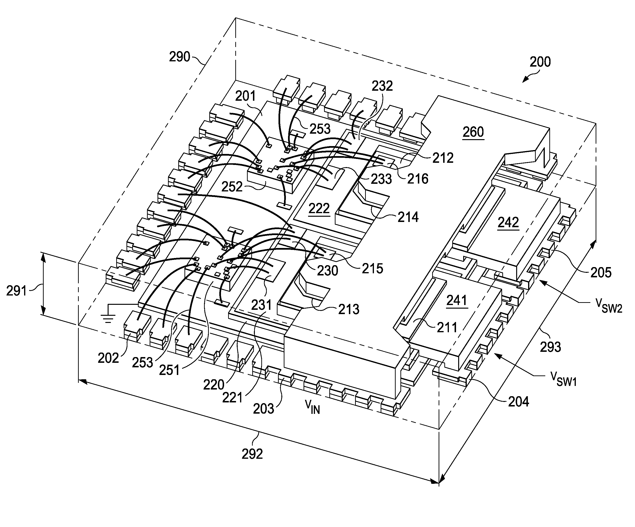
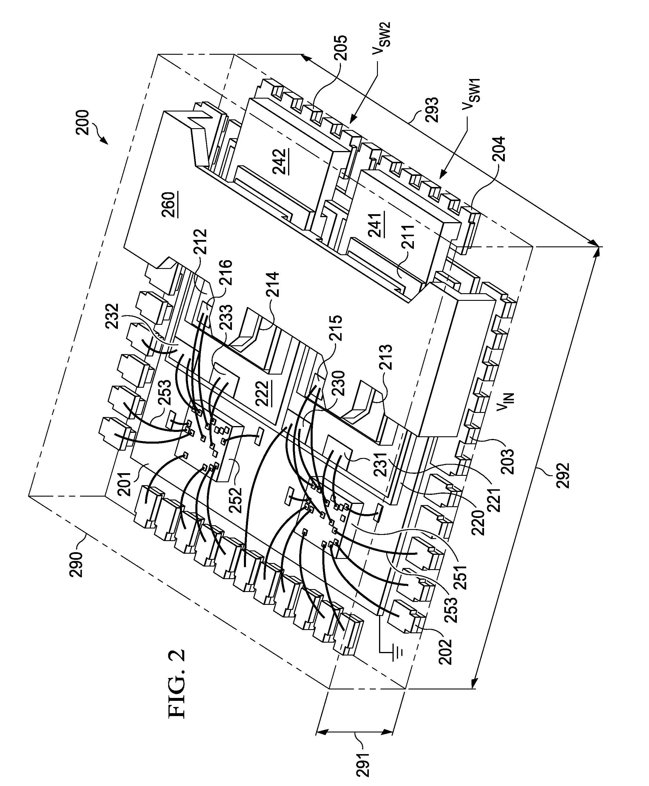
[0027]FIG. 2 illustrates a perspective view of an embodiment of a multi-output power converter generally designated 200, which is shown with a transparent encapsulation 290. Preferred actual encapsulation uses a black-colored epoxy formulation for a transfer molding technology. The exemplary converter of FIG. 2 has a length 292 of 7 mm, and a width 293 of 5 mm, and a thickness 191 of 1.0 mm. Converter 200 is constructed on a substrate, which may b...


PUM


Abstract

A packaged multi-output converter (200) comprising a leadframe with a chip pad (201) as ground terminal and a plurality of leads (202) including the electrical input terminal (203); a first FET chip (sync chip, 220) with its source terminal affixed to the leadframe and on its opposite surface a first drain terminal (221) positioned adjacent to a second drain terminal (222), the drain terminals connected respectively by a first (241) and a second (242) metal clip to a first (204) and second (205) output lead; a second FET chip (control chip, 211), positioned vertically over the first drain terminal, with its source terminal attached onto the first clip; a third FET chip (control chip, 212), positioned vertically over the second drain terminal, with its source terminal attached onto the second clip; and the drain terminals (213, 214) of the second and third chips attached onto a third metal clip (260) connected to the input lead (203).

Description

[0001]This application claims priority to Provisional Application No. 61 / 810,860 filed on Apr. 11, 2013.FIELD OF THE INVENTION[0002]The present invention is related in general to the field of semiconductor devices and processes, and more specifically to the structure and fabrication method of multi-phase half-bridges and multi-output power switches with vertically stacked semiconductor chips, especially of different down-terminal types.DESCRIPTION OF RELATED ART[0003]Among the popular families of power supply circuits are the power switching devices for converting one DC voltage to another DC voltage. Particularly suitable for the emerging power delivery requirements are the Power Blocks with two power MOS field effect transistors (FETs) connected in series and coupled together by a common switch node; such assembly is also called a half bridge. When a regulating driver and controller is added, the assembly is referred to as Power Stage or, more commonly, as synchronous Buck convert...

Claims


Application Information

Patent Timeline
Patent Type & Authority Patents(United States)
IPC IPC(8): H01L23/495H01L23/00H01L23/498
CPCH01L23/49524H01L23/49562H01L23/49575H01L24/34H01L23/49838H01L2224/32245H01L2224/48091H01L2224/48137H01L2224/48247H01L2924/1301H01L2924/1305H01L2924/1306H01L2924/13091H01L2924/15747H01L2924/00014H01L2924/00H01L2924/181H01L2224/40245H01L24/40H01L2224/40139H01L2224/73221H01L2224/40095H01L2924/15724H01L2224/8484H01L2224/84801H01L24/29H01L24/32H01L24/37H01L24/38H01L24/41H01L24/45H01L24/48H01L24/49H01L24/97H01L2224/37147H01L2224/45014H01L2224/45015H01L2224/45144H01L2224/45147H01L2224/73263H01L2224/73265H01L2224/83191H01L2924/10272H01L2924/10329H01L2924/1033H01L2924/1576H01L2224/29101H01L2224/8485H01L24/84H01L2224/0603H01L2924/01028H01L2924/014H01L2924/20752H01L2924/00012H01L2924/206H01L2224/40137H01L24/36H01L21/50H01L25/0657H01L25/072H01L25/16H01L25/18H01L25/50H01L2224/40145H01L21/561
Inventor DENISON, MARIECARPENTER, BRIAN ASHLEYLOPEZ, OSVALDO JORGEHERBSOMMER, JUAN ALEJANDRONOQUIL, JONATHAN
Owner TEXAS INSTR INC
Why Eureka
Try Eureka