Display panel and display module

A display panel and display module technology, applied in nonlinear optics, instruments, optics, etc., can solve the problems of metal fan-out wiring disconnection, shrinking space, affecting the touch function of the panel, etc., to increase the wiring width, increase The effect of total width

Inactive Publication Date: 2019-04-02
WUHAN CHINA STAR OPTOELECTRONICS TECH CO LTD
View PDF11 Cites 10 Cited by
  • Summary
  • Abstract
  • Description
  • Claims
  • Application Information

AI Technical Summary

Problems solved by technology

Due to the continuous improvement of the current display screen ratio, the lower border of the display panel (lower border) is getting smaller and smaller, resulting in the panel connecting the output pin (output pin) of the interlace integrated chip (Interlace IC) and the display (Active Area, AA) The space of the metal fan-out (Fanout) routing of the touch signal line and the data signal line in the area is reduced (inter

Method used


Image

  • Display panel and display module
  • Display panel and display module
  • Display panel and display module

Examples


Embodiment Construction

[0027] In order to further explain the technical means adopted by the present invention and its effects, the following describes in detail the preferred embodiments of the present invention and the accompanying drawings.

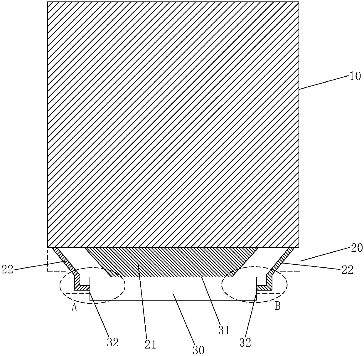
[0028] See Figure 1 to Figure 3 , The present invention provides a display panel including: a display area 10, a driving chip 30 located on one side of the display area 10, and a fan-out wiring area 20 connecting the display area 10 and the driving chip 30;

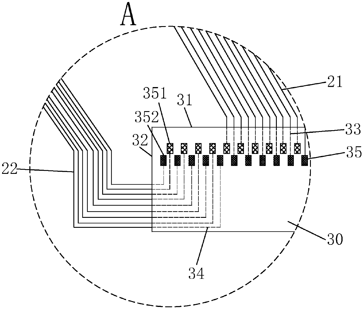
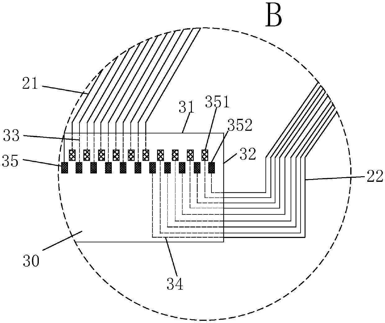
[0029] The driving chip 30 includes a first side 31 and two second sides 32 vertically connected to both ends of the first side 31;

[0030] The fan-out wiring area 20 includes a plurality of first fan-out wirings 21 connected to the first side 31 and a plurality of second fan-out wirings 22 respectively connected to the two second sides 32.

[0031] It should be noted that the driving chip 30 of the present invention includes a first side 31 and two second sides 32 perpendicularly connected to both ends of th...


PUM


Abstract

The invention provides a display panel and a display module. The display panel includes a display area, a driving chip located on one side of the display area, and a fan-out trace area connecting thedisplay area and the driving chip. The driving chip includes a first side, and two second sides vertically connected to two ends of the first side, respectively. The fan-out trace area includes a plurality of first fan-out traces connected to the first side, and a plurality of second fan-out traces respectively connected to the two second sides. According to the display panel and the display module, several signals of the driving chip are transmitted from the second sides at the two sides of the driving chip to the display area through the plurality of second fan-out traces, thereby increasingthe total width of the fan-out trace area so as to increase the width of the traces in the fan-out trace area to avoid the risk of trace breakage and reduce the impedance of the traces.

Description

Technical field [0001] The present invention relates to the field of display technology, in particular to a display panel and a display module. Background technique [0002] Thin Film Transistor (TFT) is the main driving element in current liquid crystal display (Liquid Crystal Display, LCD) and Active Matrix Organic Light-Emitting Diode (AMOLED), directly It is related to the display performance of the flat panel display device. [0003] Most of the liquid crystal displays on the current market are backlit liquid crystal displays, which include a liquid crystal display panel and a backlight module. The working principle of the liquid crystal display panel is to inject liquid crystal molecules between the ThinFilm Transistor Array Substrate (TFT Array Substrate) and the Color Filter (CF) substrate, and apply pixel voltages on the two substrates. And the common voltage, the rotation direction of the liquid crystal molecules is controlled by the electric field formed between the pi...

Claims


Application Information

Patent Timeline
IPC IPC(8): G02F1/1345
CPCG02F1/13452
Inventor 卢延涛
Owner WUHAN CHINA STAR OPTOELECTRONICS TECH CO LTD
Why Eureka
Try Eureka