Trimmer impedance component, semiconductor device and trimming method

a technology of impedance component and trimmer, which is applied in the direction of semiconductor devices, semiconductor/solid-state device details, adjustable resistors, etc., can solve the problems of product defects, inability to recover trimming, and inability to accurately trim the impedance, so as to achieve accurate and stable operation to the high-frequency signal, accurate trimming

Inactive Publication Date: 2007-04-17
SHARP KK
View PDF8 Cites 11 Cited by
  • Summary
  • Abstract
  • Description
  • Claims
  • Application Information

AI Technical Summary

Benefits of technology

[0011]Accordingly, the object of the present invention is to provide a trimmer impedance component capable of preventing the parasitic impedance between the component and a semiconductor layer from changing when impedance is trimmed and obtaining the desired impedance value even to a high-frequency signal.

Problems solved by technology

In general, the resistance value of a resistor formed through semiconductor processes disadvantageously has its absolute value varied by about ±10% due to the influences of variations in processing heat treatment, variations in the implantation energy and dosage during ion implantation and variations in processing dimensions (particularly linewidth) attributed to a photoetching process.
The variations in the resistance value of the resistor disadvantageously directly influence the output voltage and so on of the semiconductor device.
Therefore, almost all the semiconductor integrated circuit products provided with constant-voltage power supply circuits capable of adjusting the generated voltage have been subjected to trimming, and the trimming cannot be recovered once the trimming is carried out.
For the about reasons, there is a concern that the product might be defective through the re-measurement after the trimming.
In order to avoid this occurrence, a method for making a gradual approach to the expected value by repeating the measurement and trimming again and again cannot help being taken, and time required for the trimming has been long.
For example, in the aforementioned semiconductor integrated circuit, a p-type diffusion layer formed on an n-type epitaxial layer is cut, so that a parasitic capacitance between the n-type epitaxial layer and the p-type diffusion layer (trimmer resistors) changes depending on the portion trimmed, and the characteristics to the high-frequency signal change, disadvantageously causing a harmful influence of, for example, phase shift.

Method used


Image

  • Trimmer impedance component, semiconductor device and trimming method
  • Trimmer impedance component, semiconductor device and trimming method
  • Trimmer impedance component, semiconductor device and trimming method

Examples


first embodiment

[0062](The First Embodiment)

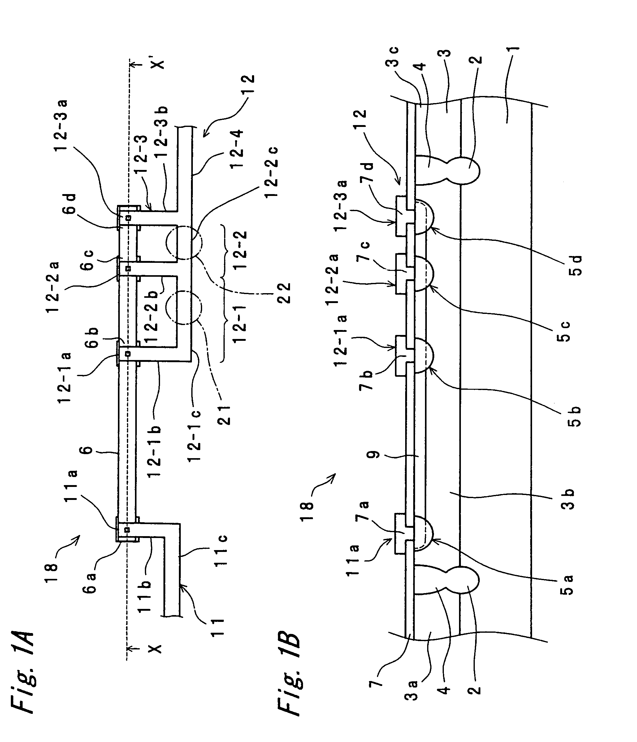
[0063]A semiconductor device including the trimmer impedance component of this invention will be described as the first embodiment with reference to FIGS. 1A and 1B. FIG. 1B is a sectional view taken along the line X–X′ in FIG. 1A.

[0064]The manufacturing method of the semiconductor device of this first embodiment is now described. First of all, a p-type embedded diffusion layer 2 for element isolation is formed on the surface of a p-type semiconductor substrate 1. Next, an n-type epitaxial layer 3 is formed on the entire surface of the p-type semiconductor substrate 1, and a p-type isolated diffusion layer 4 is formed in a portion corresponding to the p-type embedded diffusion layer 2 from the surface of the n-type epitaxial layer 3. As a result, the n-type epitaxial layer 3 is electrically divided into a plurality of portions, so that the active components of transistors or the passive components of diffused resistors and capacitors are formed at the res...

second embodiment

[0083](The Second Embodiment)

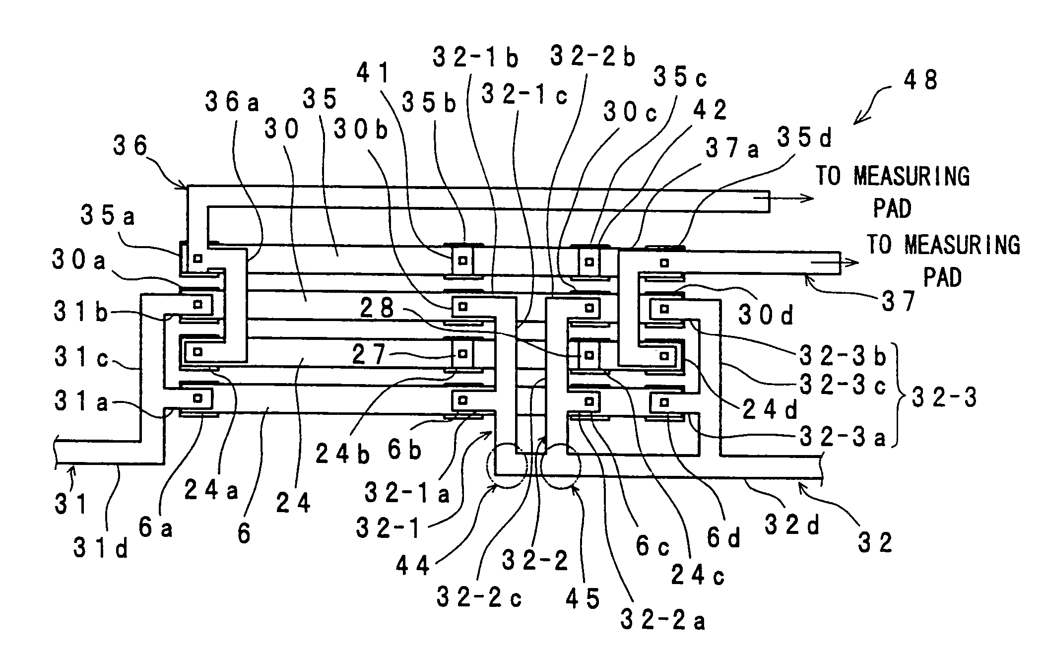
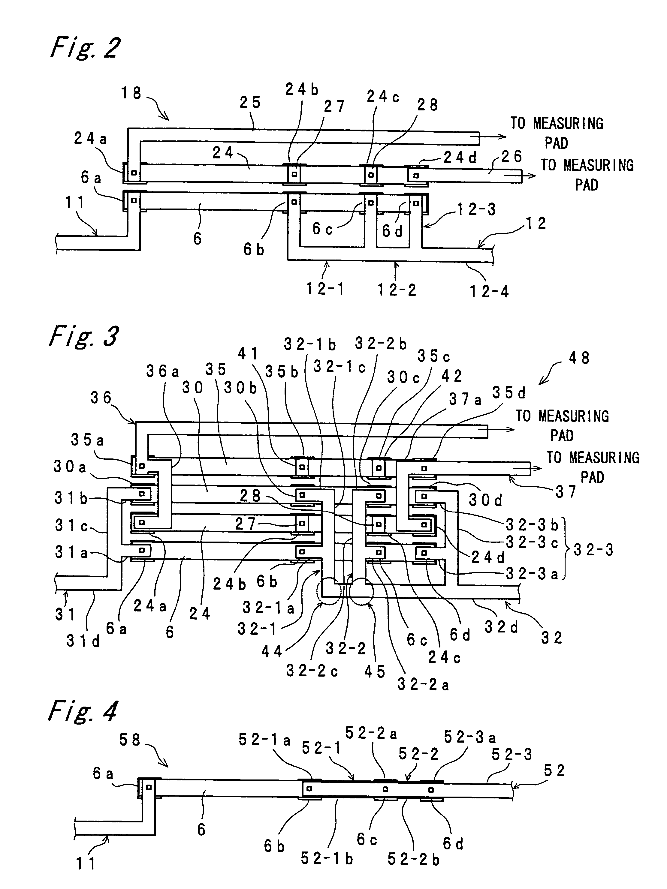
[0084]Next, the second embodiment of the semiconductor device of this invention is shown in FIG. 3. This second embodiment differs from the aforementioned first embodiment in the following points of (i) through (iv).

[0085](i) A trimmer resistance component 48 that has a trimmer resistor 6 and a trimmer resistor 30 is provided in place of the trimmer resistance component 18.

[0086](ii) A first electrode 31 and a second electrode 32 connected to the trimmer resistors 6 and 30 are provided in place of the first electrode 11 and the second electrode 12 connected to the trimmer resistor 6.

[0087](iii) A monitor resistor 35 is provided in addition to the monitor resistor 24.

[0088](iv) A first electrode 36 and a second electrode 37 connected to the monitor resistors 24 and 35 are provided in place of the first electrode 25 and the second electrode 26 connected to the monitor resistor 24.

[0089]This second embodiment is similar to the first embodiment in that the m...

third embodiment

[0104](The Third Embodiment)

[0105]FIG. 4 shows the third embodiment of the semiconductor device of this invention. This third embodiment differs from the first embodiment in that a trimmer resistance component 58 having a second electrode 52 is provided in place of the second electrode 12.

[0106]This second electrode 52 is formed on the trimmer resistor 6. This second electrode 52 has a first connection portion 52-1, a second connection portion 52-2 and a third connection portion 52-3. An end portion 52-1a of this first connection portion 52-1 is connected to the portion 6b of the trimmer resistor 6, and an end portion 52-2a of the second connection portion 52-2 is connected to the portion 6c of the trimmer resistor 6. Moreover, an end portion 52-3a of the third connection portion 52-3 is connected to the portion 6d of the trimmer resistor 6. Moreover, the second electrode 52 is linearly extended in the lengthwise direction, while the first connection portion 52-1, the second connect...


PUM


Abstract

A trimmer resistance component of the present invention has a trimmer resistor constructed of a p-type diffusion layer formed on the surface of an n-type epitaxial layer. A first electrode is connected to a portion located on one end side of this trimmer resistor, while a first connection portion, a second connection portion and a third connection portion of the second electrode are connected to portions located on the other end side. By cutting a portion of the first connection portion and a portion of the second connection portion by laser trimming, a resistance value between the first electrode and the second electrode can be trimmed without changing a parasitic capacitance between the trimmer resistor and the n-type epitaxial layer.

Description

[0001]This Nonprovisional application claims priority under 35 U.S.C. §119(a) on Patent Application No. 2003-393817 filed in Japan on Nov. 25, 2003, the entire contents of which are hereby incorporated by reference.BACKGROUND OF THE INVENTION[0002]This invention relates to a trimmer impedance component, a semiconductor device and a trimming method and relates, in particular, to a semiconductor device with a built-in high-speed element as one example and laser trimming that is a trimming method for obtaining a high-accuracy resistance value.[0003]In general, the resistance value of a resistor formed through semiconductor processes disadvantageously has its absolute value varied by about ±10% due to the influences of variations in processing heat treatment, variations in the implantation energy and dosage during ion implantation and variations in processing dimensions (particularly linewidth) attributed to a photoetching process.[0004]The variations in the resistance value of the resi...

Claims


Application Information

Patent Timeline
Patent Type & Authority Patents(United States)
IPC IPC(8): H01C10/00H01L21/3205H01L21/822H01L23/52H01L27/04H01L27/08
CPCH01L27/0802
Inventor FUKUNAGA, NAOKI
Owner SHARP KK
Why Eureka
Try Eureka