
Semiconductor manufacturing system

a manufacturing system and semiconductor technology, applied in the field of semiconductor semiconductor manufacturing system, can solve the problems of imposing a burden on the operator, affecting the efficiency of series inspection operations, and easy to cause manipulation errors, so as to reduce the load on the environment, prevent operation errors, and perform inspection operations very efficiently

Active Publication Date: 2015-12-29
TOKYO ELECTRON LTD
View PDF15 Cites 1 Cited by
  • Summary
  • Abstract
  • Description
  • Claims
  • Application Information

AI Technical Summary

Benefits of technology

The system significantly reduces operator errors and increases inspection efficiency by automating inspection processes, while minimizing environmental impact by eliminating paper-based workflows.

Problems solved by technology

Accordingly, since the operator needs to pay great attention, it may impose a burden on the operator.
Further, a manipulation error is easily likely to occur.
Further, when there are mixed manipulation / checkup operations to be performed through the screen and manipulation / checkup operations to be performed directly or manually by the operator, a series of inspection operations may not be performed with high efficiency and it may take great time to complete the inspection.
Since, however, the workflow chart for the conventional inspection operation is printed on a paper, a load on the environment is caused.

Method used


Image

  • Semiconductor manufacturing system
  • Semiconductor manufacturing system
  • Semiconductor manufacturing system

Examples


Embodiment Construction

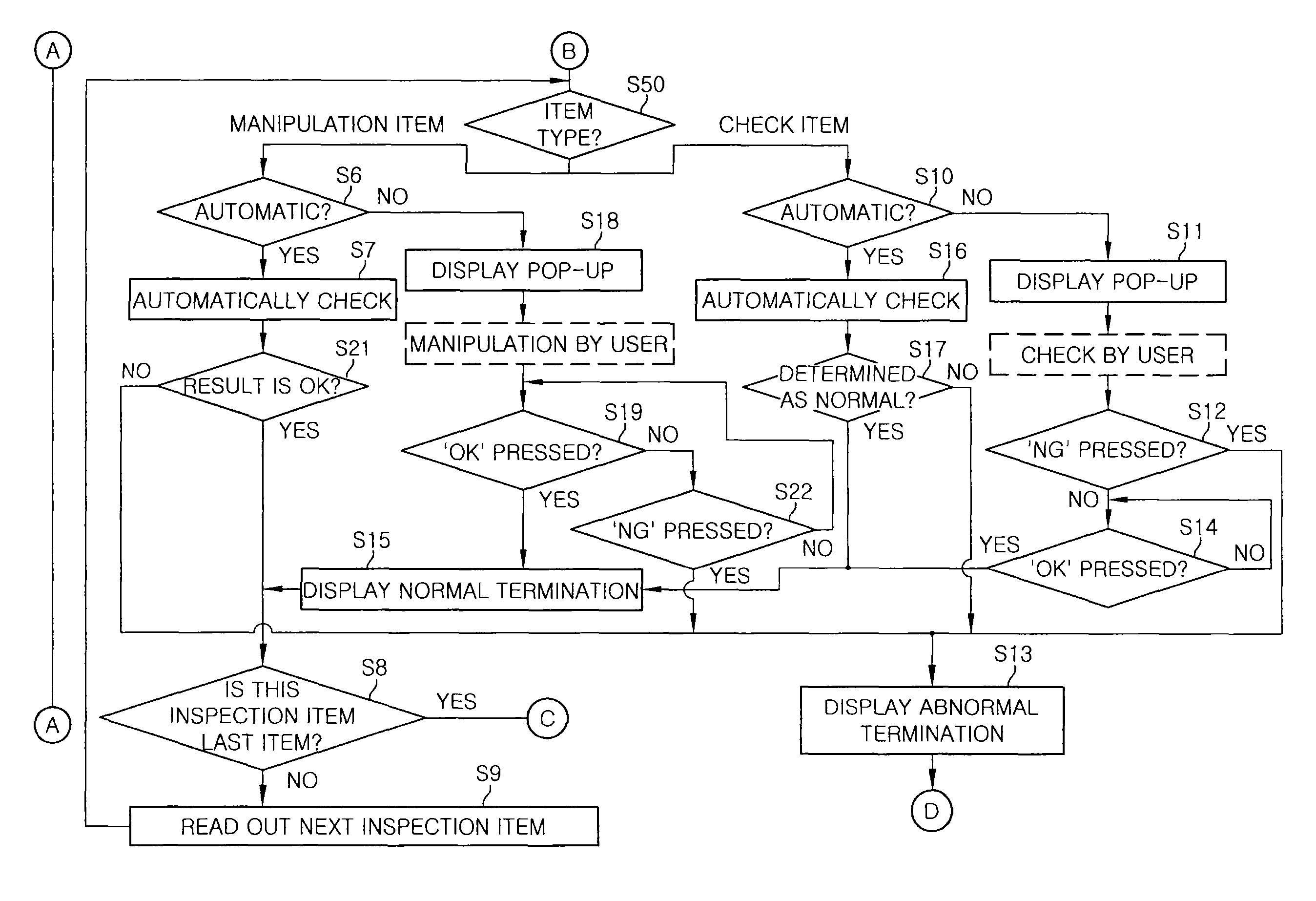
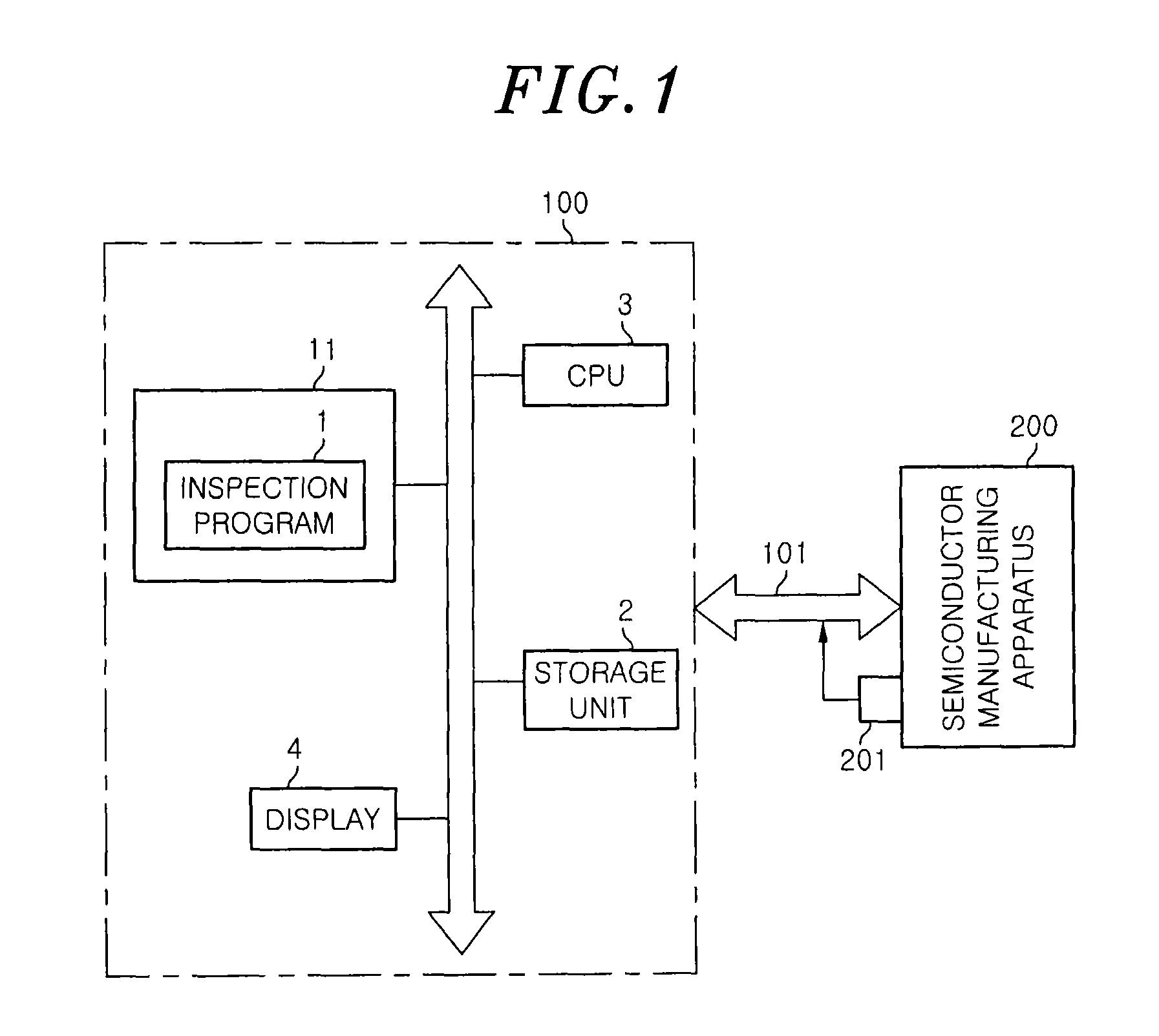
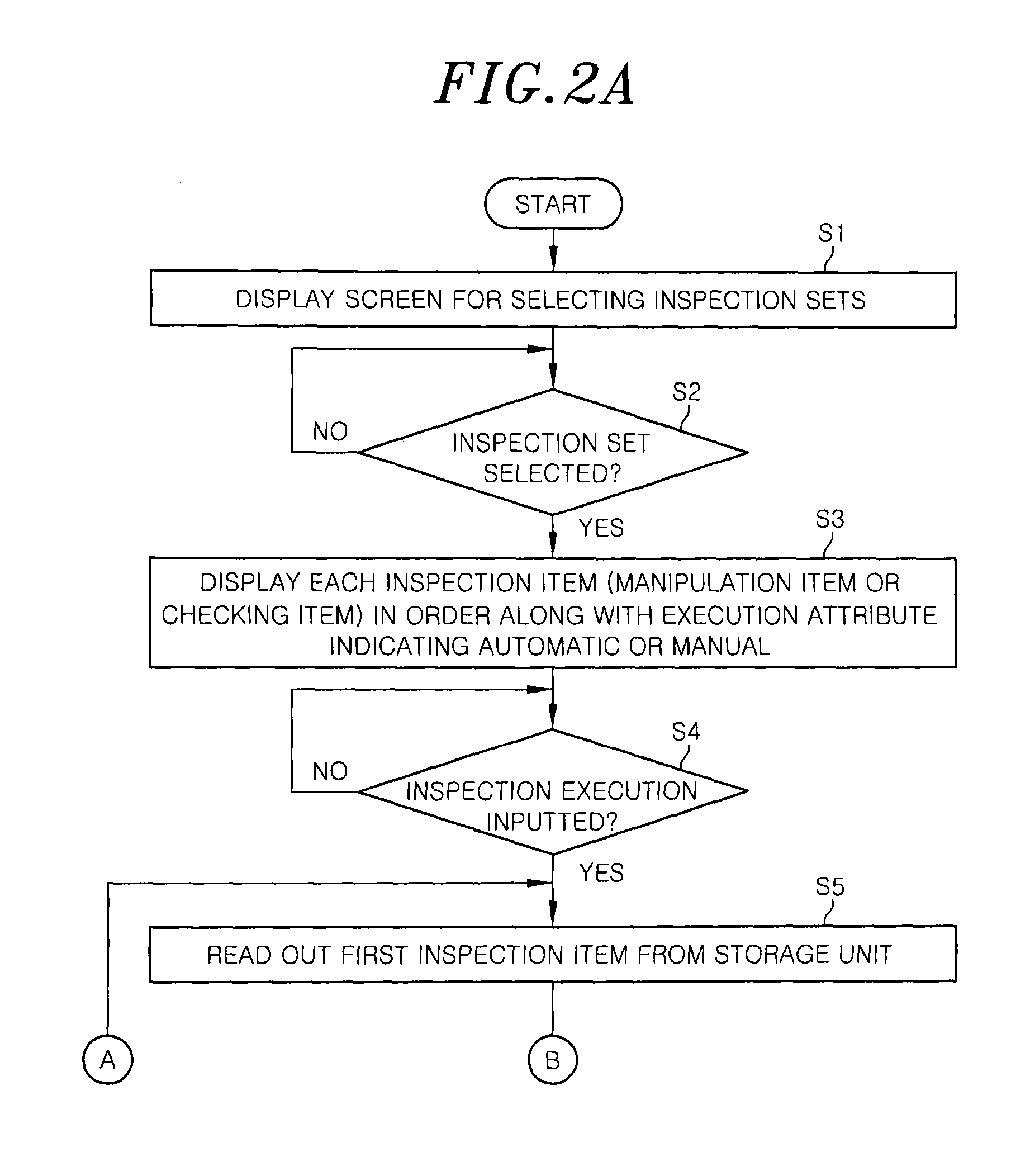
[0055]FIG. 1 is a schematic diagram showing an overall configuration of a semiconductor manufacturing system in accordance with a first embodiment of the present invention. In FIG. 1, a reference numeral ‘100’ denotes a control unit including a computer and a reference numeral ‘200’ represents a semiconductor manufacturing apparatus controlled by the control unit 100. The control unit 100 includes a program storage 11 in which an inspection program 1 is stored and also includes a storage unit 2, a CPU 3 and a display 4. The control unit 100 may include a computer provided for each semiconductor manufacturing apparatus or a host computer for controllers of a plurality of semiconductor manufacturing apparatuses. The control unit 100 outputs a control signal for controlling devices in the semiconductor manufacturing apparatus 200 through a signal line 101. A detector 201 in the semiconductor manufacturing apparatus 200 sends a measurement result and a detection result indicating an ope...


PUM

PropertyMeasurementUnit
voltageaaaaaaaaaa
voltageaaaaaaaaaa
voltageaaaaaaaaaa

Abstract

A semiconductor manufacturing system includes circuitry configured to execute: displaying a screen for selecting an inspection set including inspection items having a manipulation item and / or a check item; retrieving the inspection items, arranging the inspection items in the order of workflow, and displaying each inspection item on a screen with an execution attribute indicating whether each inspection item is “automatic” or “manual” execution; receiving an inspection start command and reading the first inspection item from a storage unit. The circuitry also executes steps corresponding to the following cases (a) to (d) until there are no more inspection items: (a) the read-out inspection item being the manipulation item and “automatic”; (b) the read-out inspection item being the manipulation item and “manual”; (c) the read-out inspection item being the check item and “automatic”; and (d) the read-out inspection item being the check item and “manual”.

Description

[0001]This application is a Continuation Application of PCT International Application No. PCT / JP2011 / 056238 filed on Mar. 16, 2011, which designated the United States.FIELD OF THE INVENTION[0002]The present invention relates to a semiconductor manufacturing system including a program for inspecting a semiconductor manufacturing apparatus.BACKGROUND OF THE INVENTION[0003]For example, when performing an inspection process before a semiconductor manufacturing apparatus is shipped or when performing maintenance of the semiconductor manufacturing apparatus by a user, the content of the inspection operation is previously defined in order to improve safety of the apparatus and an operator, and to improve processing efficiency while guaranteeing the quality of the apparatus. Specifically, the inspection operation may include manipulating component devices of the semiconductor manufacturing apparatus or checking the result of the manipulation.[0004]Examples of the inspection operation may be...

Claims


Application Information

Patent Timeline
Patent Type & Authority Patents(United States)
IPC IPC(8): G01N21/88G06F3/00G01N21/95G01N21/75G05B19/4065
CPCG05B19/4065G05B2219/32226Y02P90/02H01L21/02008H01L21/0273H01L21/30655H01L21/67718
Inventor IKEDA, GAKUMIYASHITA, KOICHICHIKUMA, TAKAMASAGOMI, SATOSHILI, CHUNMUITAKANO, KUNIO
Owner TOKYO ELECTRON LTD
Learn More