Contaminant measurement substrate, apparatus and method for fabricating substrate using the same

a technology of contaminant measurement and substrate, which is applied in the direction of instruments, transportation and packaging, material analysis, etc., can solve the problems of inferiority of the substrate of the display device that is fabricated as a completed product, and achieve the effect of effectively preventing and effectively preventing the inferiority of the substra

Active Publication Date: 2016-02-23
SAMSUNG DISPLAY CO LTD
View PDF6 Cites 0 Cited by
  • Summary
  • Abstract
  • Description
  • Claims
  • Application Information

AI Technical Summary

Benefits of technology

[0010]Exemplary embodiments of the invention provide a contaminant measurement substrate, which can effectively prevent inferiority of a substrate that passes through actual processes, using measuring of contaminants of a chamber before the actual processes of the substrate, grasping of the occurrence position of the contaminants and removing of the occurrence cause of the contaminants.
[0011]Another exemplary embodiment of the invention provide an apparatus for fabricating a substrate, which can effectively prevent inferiority of a substrate that passes through actual processes, using measuring of contaminants of a chamber before the actual processes of the substrate, grasping of the occurrence position of the contaminants and removing of the occurrence cause of the contaminants.
[0012]Another exemplary embodiment of the invention provide a method for fabricating a substrate, which can effectively prevent inferiority of a substrate that passes through actual processes, by measuring of contaminants of a chamber before the actual processes of the substrate, grasping of the occurrence position of the contaminants and removing of the occurrence cause of the contaminants.
[0016]According to exemplary embodiments of the invention, at least the following effects can be achieved.
[0018]Accordingly, the contaminant measurement substrate according to an embodiment of the invention can effectively prevent the inferiority of the substrate that passes by the actual processes.

Problems solved by technology

When a number of contaminants that adsorb to a substrate for a display device exceeds a reference value, inferiority may occur in the substrate for a display device that is fabricated as a completed product.

Method used


Image

  • Contaminant measurement substrate, apparatus and method for fabricating substrate using the same
  • Contaminant measurement substrate, apparatus and method for fabricating substrate using the same
  • Contaminant measurement substrate, apparatus and method for fabricating substrate using the same

Examples


Embodiment Construction

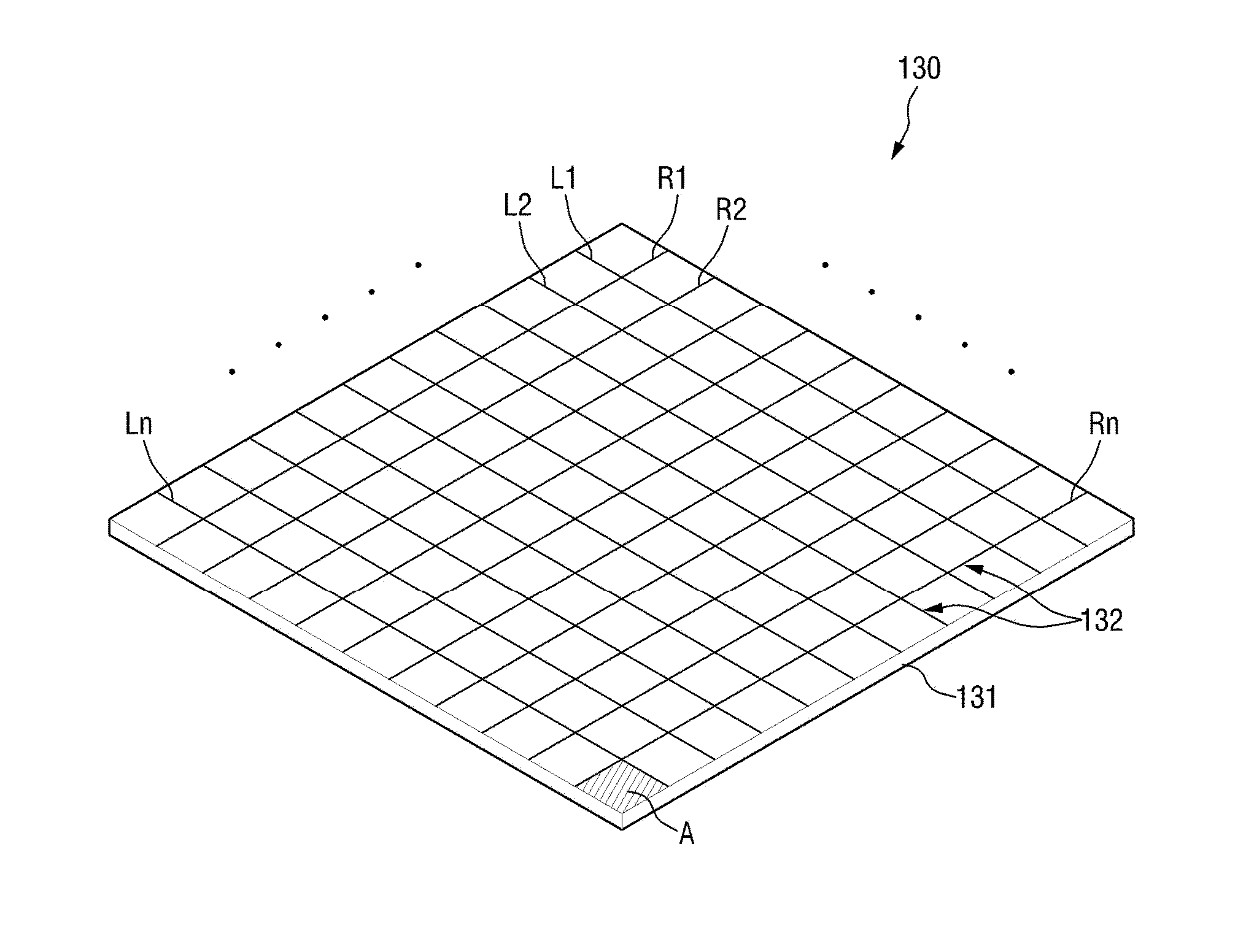
[0029]The invention now will be described more fully hereinafter with reference to the accompanying drawings, in which various embodiments are shown. This invention may, however, be embodied in many different forms, and should not be construed as limited to the embodiments set forth herein. Rather, these embodiments are provided so that this disclosure will be thorough and complete, and will fully convey the scope of the invention to those skilled in the art. Like reference numerals refer to like elements throughout.

[0030]It will also be understood that when a layer is referred to as being “on” another layer or substrate, it can be directly on the other layer or substrate, or intervening layers may also be present. The same reference numbers indicate the same components throughout the specification.

[0031]It will be understood that, although the terms first, second, third etc. may be used herein to describe various elements, components, regions, layers and / or sections, these elements...


PUM

PropertyMeasurementUnit
electrostatic polarityaaaaaaaaaa
coloraaaaaaaaaa
shapesaaaaaaaaaa

Abstract

An apparatus for fabricating a substrate includes a chamber providing a space in which processes are performed, a contaminant measurement substrate including a base material configured to collect contaminants, and laser marks on the base material and defining coordinates of the base material, a first stage disposed inside the chamber, and upon which the contaminant measurement substrate is seated during collection of the contaminants of the chamber, a second stage disposed outside the chamber, and upon which the contaminant measurement substrate is seated during measurement of the contaminants of the chamber collected on the contaminant measurement substrate, and a contaminant measurement light source disposed on an upper portion of the second stage and configured to irradiate the contaminant measurement substrate seated on the second stage with light during the measurement of the contaminants of the chamber collected on the contaminant measurement substrate.

Description

[0001]This application claims priority to Korean Patent Application No. 10-2013-0088059, filed on Jul. 25, 2013, and all the benefits accruing therefrom under 35 U.S.C. §119, the disclosure of which is incorporated herein in its entirety by reference.BACKGROUND[0002]1. Field[0003]The invention relates to a contaminant measurement substrate, an apparatus and a method for fabricating a substrate using the same.[0004]2. Description of the Prior Art[0005]A substrate for a display device such as an organic light emitting display (“OLED”), a liquid crystal display (“LCD”), or a plasma display is fabricated as a completed product by fabricating processes.[0006]The fabricating processes include a substrate thin-film deposition process, a coating process, and an assembling process, and are performed in respective process chambers.[0007]While a substrate for a display device is processed by the fabricating processes, contaminants which occur due to splitting or aging of portions of the proces...

Claims


Application Information

Patent Timeline
Patent Type & Authority Patents(United States)
IPC IPC(8): H01L51/56H01L51/00G01N21/95G01N21/88G01N21/94
CPCG01N21/95G01N21/94H01L51/0096G01N2021/9513Y10T29/49764Y10T29/51Y10T428/24802Y02E10/549H10K77/10H10K71/00
Inventor PARK, CHONG, JIN
Owner SAMSUNG DISPLAY CO LTD
Why Eureka
Try Eureka