
Manufacturing method of electroluminescent device

a manufacturing method and electroluminescent technology, applied in the manufacture of electrode systems, instruments, electric discharge tubes/lamps, etc., can solve the problems of electroluminescent performance degradation, low luminous efficiency, and shorten the life of cathode stripping, so as to prevent the deterioration of the characteristics of the organic layer

Active Publication Date: 2006-04-25
SAMSUNG DISPLAY CO LTD
View PDF4 Cites 2 Cited by
  • Summary
  • Abstract
  • Description
  • Claims
  • Application Information

AI Technical Summary

Benefits of technology

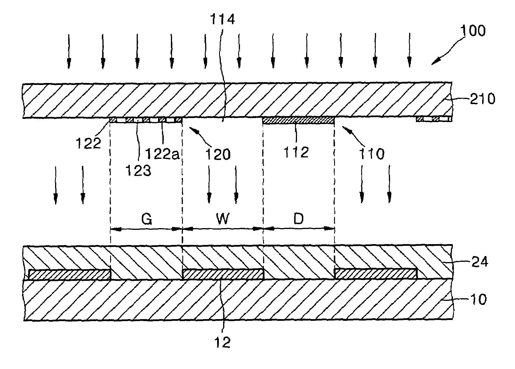
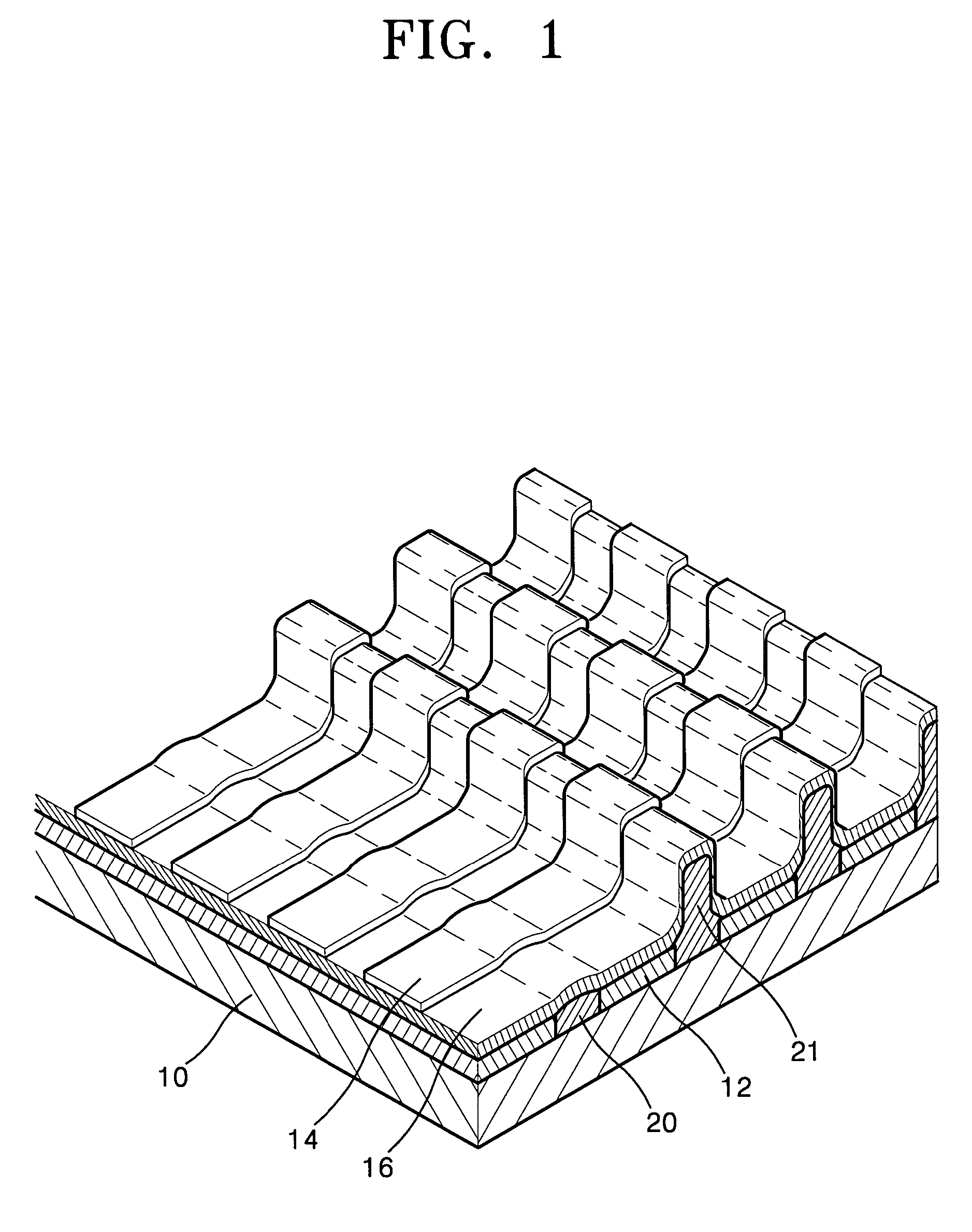
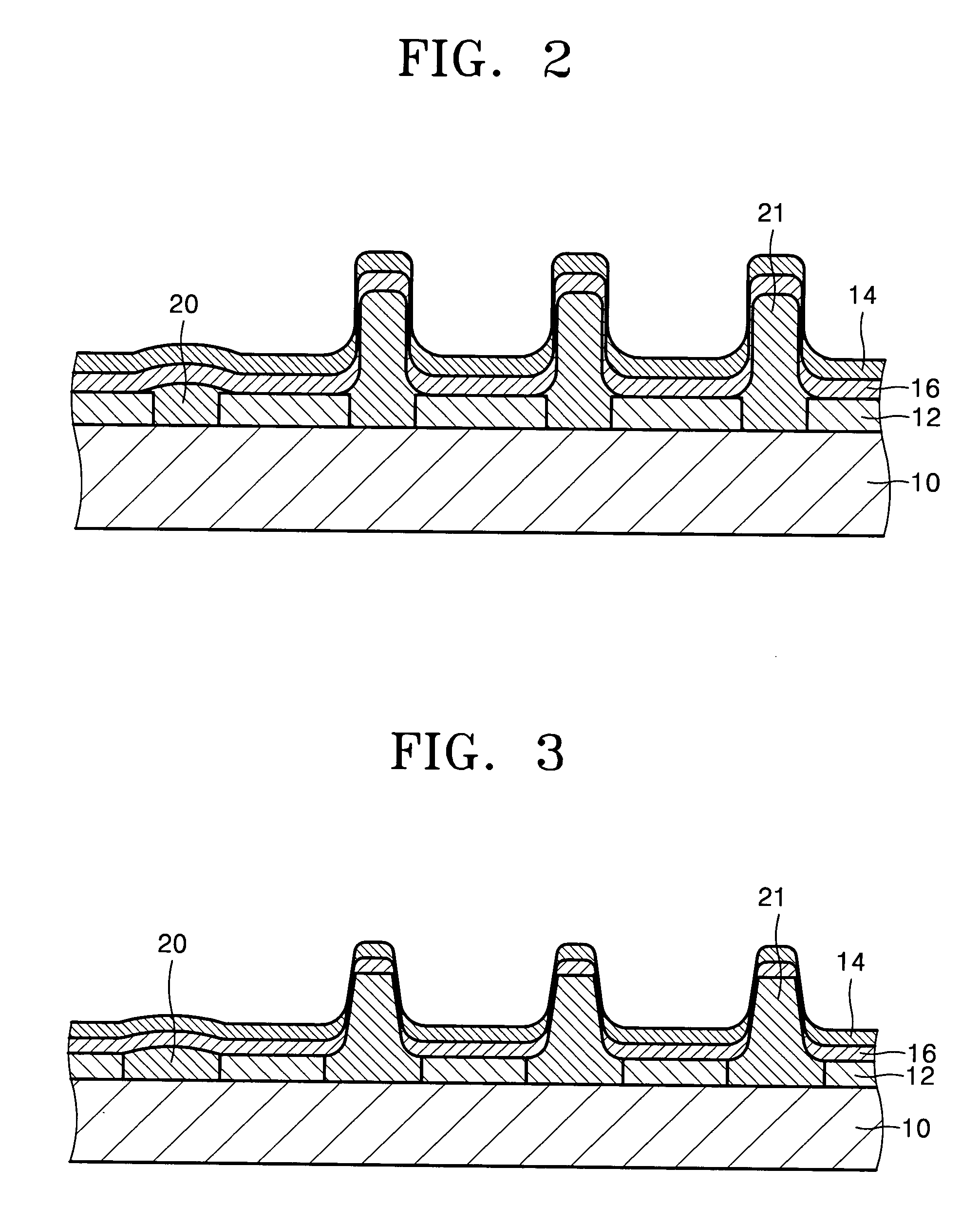
[0024]The present invention provides a method of manufacturing an electroluminescent (EL) device which can prevent layers from being damaged due to a deposition mask, can prevent a short-circuit between a first electrode and a second electrode, and can prevent deterioration of organic layer characteristics due to non-uniformity in coated thickness of organic layers by forming insulating walls when forming an electroluminescent layer or a cathode using a deposition mask.
[0025]Also, the present invention provides a method of manufacturing an EL device with a simplified structure, which can prevent contamination of the device due to spreading of an adhesive agent, and can prevent connection inferiority between a flexible PCB and electrode terminals and corrosion of exposed electrode terminals.
[0026]Further, the present invention provides a method of manufacturing an EL device with a simplified structure which can prevent moisture from infiltrating into the device through electrode terminals, and can remove moisture remaining in layers.

Problems solved by technology

If the cathode is formed by photolithography, however, there is a problem in that when the cathode is selectively etched using a photoresist, and the photoresist is stripped off or development is carried out, moisture may soak into an interface between organic layers and the cathode, resulting in degradation in electroluminescent performance due to the deteriorated characteristics of the organic layer, a low luminous efficiency, and a shortened life due to stripping of the cathode.
However, it is quite difficult to form fine patterns on a large substrate using a deposition mask.
According to this method using the shade of a separator, however, highly accurate patterning and high-speed deposition cannot be achieved under the conditions of variable deposition rates and a large amount of material deposited.
Also, since portions where cathodes are not formed corresponding to the shade exist in organic layers, these portions are susceptible to ingress of moisture, resulting in deterioration of the organic layers.
The deterioration of the organic layers may cause a short-circuit between the anodes and the cathodes.
This method also has many problems.
For example, the thin slit-shaped deposition mask may experience a sag of its central portion in a larger substrate, causing damage to organic layers or cathodes, thereby adversely affecting the yield.
The sag also makes it impossible to form cathodes having finer patterns.
However, close contact of the deposition mask may cause the organic layer to be damaged, resulting in a short-circuit between an anode and a cathode.
However, according to this method, a gap between the anode and each of the shielding walls makes the organic layer formed at the edge of the anode thinner.
Resultantly, the cathode may contact the anode at a lateral portion of the anode, causing a short-circuit between the cathode and the anode.

Method used


Image

  • Manufacturing method of electroluminescent device
  • Manufacturing method of electroluminescent device
  • Manufacturing method of electroluminescent device

Examples


Embodiment Construction

[0056]Reference will now be made in detail to the present preferred embodiments of the present invention, examples of which are illustrated in the accompanying drawings, wherein like reference numerals refer to the like elements throughout. The embodiments are described below in order to explain the present invention by referring to the figures.

[0057]The following description of preferred embodiments is directed mainly to the structure of an organic EL device in which organic compounds are used as light emission layers. However, the present invention can be applied in the same manner to an inorganic EL device using inorganic compounds as light emission layers.

[0058]As described above, according to an embodiment of the present invention, various insulating layers formed on a substrate and the first electrode, including an inter-insulator, an insulating wall, a shielding wall, a sealing portion, and a separator, are formed by a single process, thereby reducing the number of processing...


PUM


Abstract

A method of manufacturing an electroluminescent display (EL) device including forming a first electrode unit arranged in a first predetermined pattern on a substrate, simultaneously forming two or more insulating layers covering the substrate and at least portions of the first electrode unit and defining a light emitting area having a second predetermined pattern, the insulating layers having different heights and patterns, forming an electroluminescent (EL) layer on the light-emitting area, forming a second electrode unit in a third predetermined pattern on the light emitting area, and sealing the substrate.

Description

CROSS-REFERENCE TO RELATED APPLICATIONS[0001]This application claims the benefit of Korean Application No. 2002-45281, filed Jul. 31, 2002, in the Korean Intellectual Property Office, the disclosure of which is incorporated herein by reference.BACKGROUND OF THE INVENTION[0002]1. Field of the Invention[0003]The present invention relates to an electroluminescent (EL) device, and, more particularly, to a method of manufacturing an EL device which can simultaneously form various types of insulating layers on a substrate and on at least some portions of a first electrode.[0004]2. Description of the Related Art[0005]EL devices are self-emission type display devices, and much attention has recently been paid to the EL devices because they have advantageous features suitable for next generation devices, such as a wide viewing angle, a high contrast ratio, and a high response speed. EL devices are classified into inorganic EL devices and organic EL devices, according to the materials used in...

Claims


Application Information

Patent Timeline
Patent Type & Authority Patents(United States)
IPC IPC(8): H01J9/227H05B33/10H01L27/32H01L51/52H01L51/56
CPCH01L27/3283H01L51/56H01L51/5237H10K59/173H10K71/00H10K59/872H10K59/8722H05B33/10H10K50/841
Inventor KUM, KYO JOOLIM, JUNG KU
Owner SAMSUNG DISPLAY CO LTD
Learn More