Vertical field effect transistors with controlled overlap between gate electrode and source/drain contacts

a technology of vertical field effect transistor and gate electrode, which is applied in the field of semiconductor technology, can solve the problems of non-scalability of operating voltage, increase in power consumption, and ineffectiveness of traditional semiconductor design techniques, processes and materials,

Active Publication Date: 2016-03-15
IBM CORP
View PDF10 Cites 56 Cited by
  • Summary
  • Abstract
  • Description
  • Claims
  • Application Information

AI Technical Summary

Problems solved by technology

Semiconductor device scaling to smaller feature sizes for the last four decades, is facing significant challenges, such as increases in power consumption as increasing OFF-state leakage and non-scalability of the operating voltage, in pursuit of faster device performance.
Traditional semiconductor design techniques, processes and materials become ineffective as physical dimensions shrink down to the nanometer regime.

Method used


Image

  • Vertical field effect transistors with controlled overlap between gate electrode and source/drain contacts
  • Vertical field effect transistors with controlled overlap between gate electrode and source/drain contacts
  • Vertical field effect transistors with controlled overlap between gate electrode and source/drain contacts

Examples


Embodiment Construction

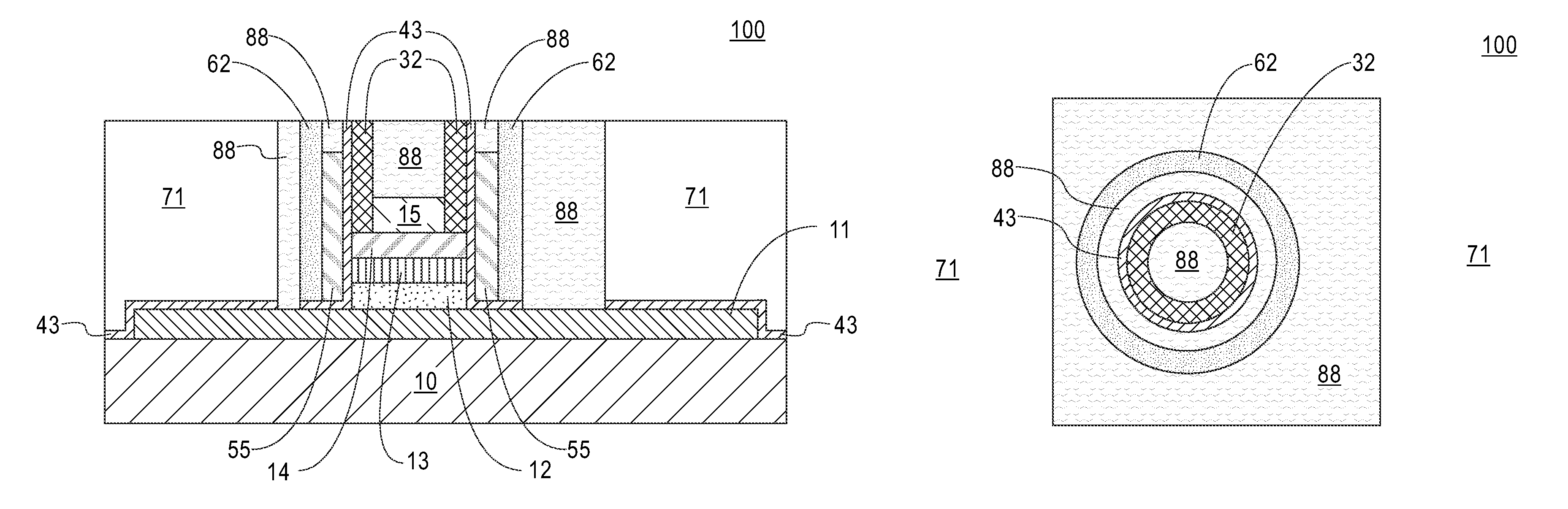
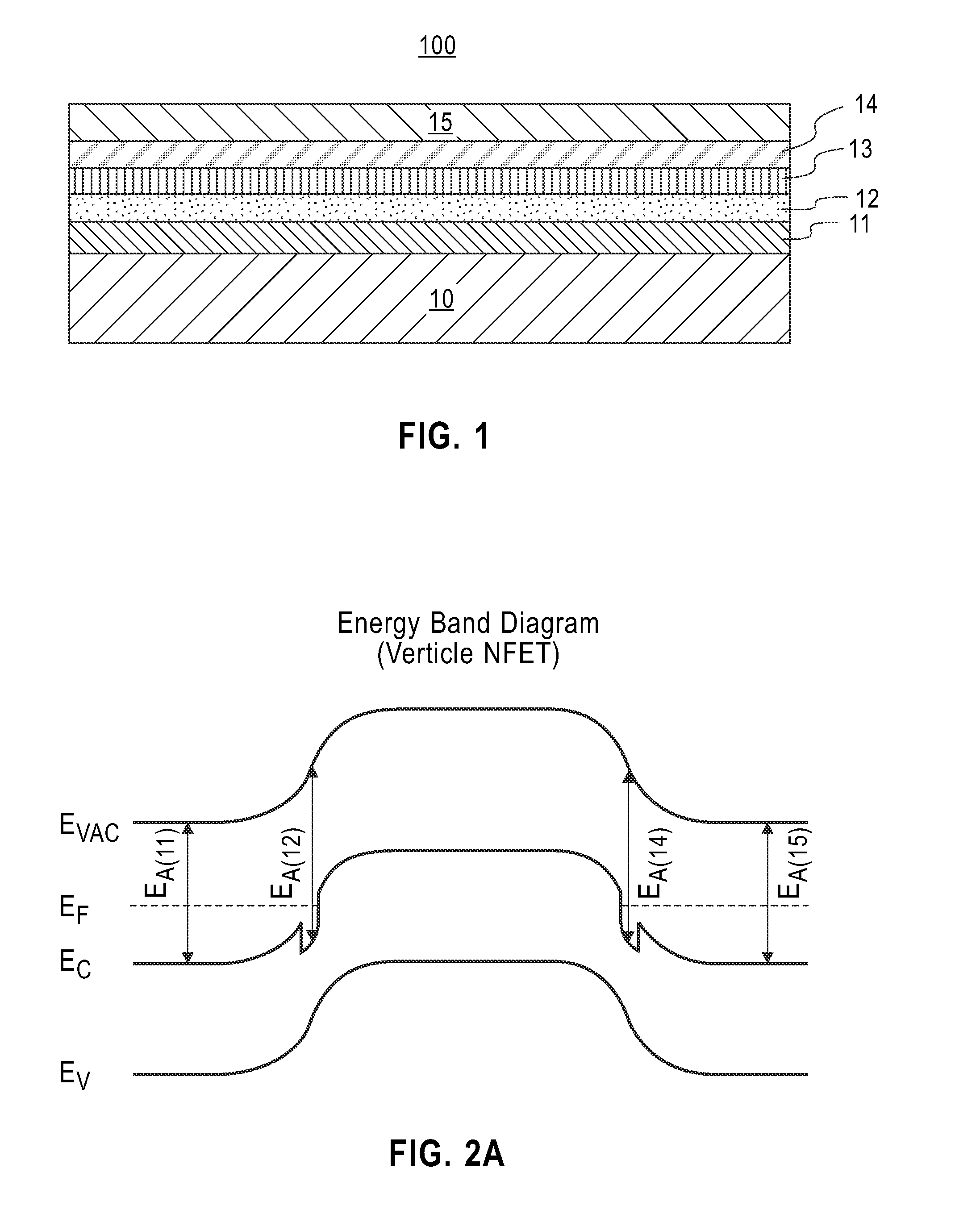
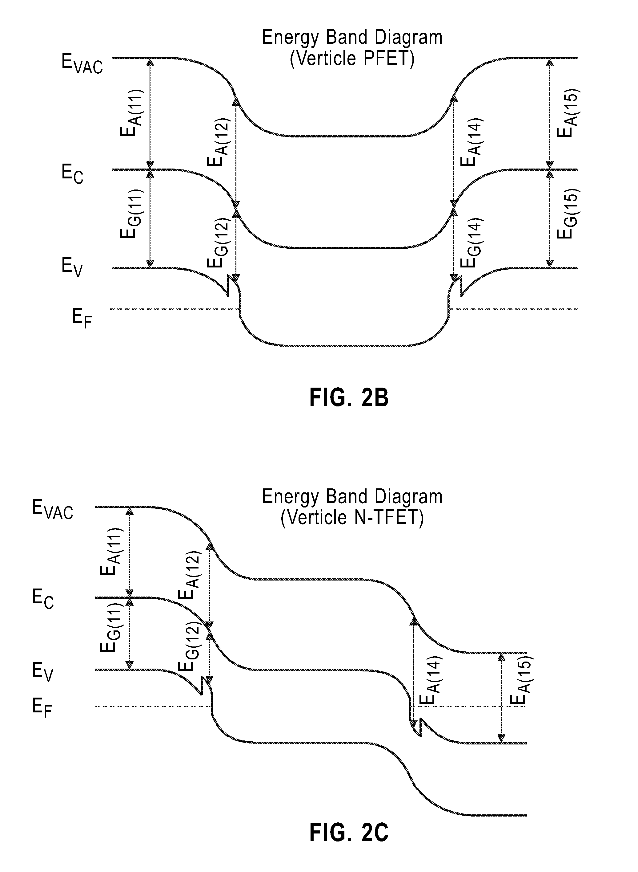
[0021]Detailed embodiments of the claimed structures and methods are disclosed herein. The method steps described below do not form a complete process flow for manufacturing integrated circuits. The present embodiments can be practiced in conjunction with the integrated circuit fabrication techniques currently used in the art, and only so much of the commonly practiced process steps are included as are necessary for an understanding of the described embodiments. The figures represent cross-section portions of a semiconductor chip or a substrate during fabrication and are not drawn to scale, but instead are drawn to illustrate the features of the described embodiments. Specific structural and functional details disclosed herein are not to be interpreted as limiting, but merely as a representative basis for teaching one skilled in the art to variously employ the methods and structures of the present disclosure. In the description, details of well-known features and techniques may be o...


PUM


Abstract

An approach to forming a semiconductor structure for a vertical field effect transistor with a controlled gate overlap. The approach includes forming on a semiconductor substrate, a first semiconductor layer, a second semiconductor layer, a third semiconductor layer, a fourth semiconductor layer, a fifth semiconductor layer, and a first dielectric layer. The etched first dielectric layer and a first drain contact are surrounded by a first spacer. The first drain contact is composed of the fifth semiconductor layer. A second drain contact composed of the fourth semiconductor layer, a channel composed of the third semiconductor layer, and a second source contact composed of the second semiconductor layer are formed. Additionally, first source contact composed of the first semiconductor is formed and a gate electrode is formed on a portion of the first source contact layer surrounding a portion of the first pillar and the second pillar.

Description

BACKGROUND OF THE INVENTION[0001]The present invention relates generally to the field of semiconductor technology, and more particularly to semiconductor structures controlling overlap between gate and source / drain contacts in vertical gate-all-around field effect transistors.[0002]Semiconductor device scaling to smaller feature sizes for the last four decades, is facing significant challenges, such as increases in power consumption as increasing OFF-state leakage and non-scalability of the operating voltage, in pursuit of faster device performance. Traditional semiconductor design techniques, processes and materials become ineffective as physical dimensions shrink down to the nanometer regime. The use of gate-all-around metal-oxide semiconductor field effect transistors (MOSFETs) with small area of cross-section gives rise to be better electrostatic control of the channel and thus, leads to lower OFF-state leakage current.[0003]In response to the challenges creating electron barrie...

Claims


Application Information

Patent Timeline
Patent Type & Authority Patents(United States)
IPC IPC(8): H01L29/775H01L21/321H01L21/28H01L29/66H01L29/15H01L29/78
CPCH01L29/152H01L29/7827H01L29/66553H01L29/66666H01L21/3212H01L21/28026H01L29/7391H01L29/42392H01L29/66742H01L29/78642H01L29/66977H01L29/78696
Inventor BASU, ANIRBANCHENG, CHENG-WEIHAENSCH, WILFRIED E.MAJUMDAR, AMLANSHIU, KUEN-TING
Owner IBM CORP
Why Eureka
Try Eureka