Metal contact for chip packaging structure

a technology of metal contact and chip packaging, applied in the field of semiconductor technology, can solve the problems of affecting the mechanical strength and service life of welded points, the chip cost decreases significantly, and the chip size decreases, so as to prevent the generation of intermetallic compounds, increase the contact area, and enhance the adhesion

Active Publication Date: 2016-03-22
NANTONG FUJITSU MICROELECTRONICS
View PDF105 Cites 6 Cited by
  • Summary
  • Abstract
  • Description
  • Claims
  • Application Information

AI Technical Summary

Benefits of technology

[0008]In embodiments of the present disclosure, the adhesion between a solder ball and a sub-ball metal electrode may be enhanced, which improves the reliability of a chip package structure.
[0029]Compared with existing techniques, the present disclosure may have following advantages. The solder ball has the first apron structure which covers a portion of the pad around the bottom of the sub-ball metal electrode. The first apron structure increases the contact area between the solder ball and the metal pad, and enhances the adhesion between the solder ball and the metal pad, such that the solder ball is not prone to fall off the metal pad under an external force.
[0030]Further, the covering layer includes the anti-diffusion layer and the wetting layer, wherein the anti-diffusion layer is disposed on the surface of the sub-ball metal electrode, and the wetting layer is disposed on the surface of the anti-diffusion layer. In the existing techniques, a solder ball is directly formed on a sub-ball metal electrode, thus, intermetallic compounds and cavities may be formed between the sub-ball metal electrode and the solder ball due to the diffusion of atoms. The intermetallic compounds are fragile, which may affect the mechanical strength and service life of welded points. In embodiments of the present disclosure, the anti-diffusion layer made of nickel is formed on the surface of the sub-ball metal electrode, which can act as a barrier layer between the sub-ball metal electrode and the solder ball to prevent the generation of intermetallic compounds and cavities. Further, the anti-diffusion layer is prone to be oxidized, thus, the wetting layer is formed on the anti-diffusion layer to prevent the oxidization of the anti-diffusion layer. The wetting layer may be infiltrated with the solder ball to be formed to lead to better adhesion. The wetting layer includes one selected from tin, gold and silver, or alloy of gold, cooper or silver. Therefore, the covering layer formed on the sub-ball metal electrode avoids the generation of intermetallic compounds, and improves the reliability of chip packaging. The second apron structure increases the contact area between the covering layer and the metal pad, and enhances the adhesion among the solder ball, the covering layer, the sub-ball metal electrode and the metal pad.
[0031]Further, the sub-ball metal electrode include the main body and the end portion, wherein the main body is the lower portion of the sub-ball metal electrode which is connected with the metal pad, and the end portion is the upper portion of the sub-ball metal electrode. The end portion enters into the solder ball, thereby increasing the contact area between the sub-ball metal electrode and the solder ball. In this way, the adhesion between the sub-ball metal electrode and the solder ball is enhanced, when suffering an external force, the solder ball is not prone to fall off the sub-ball metal electrode. Further, the sub-ball metal electrode is formed by a wire bonding process, including: bonding a metal wire with the metal pad to form the main body; the metal wire generating an arc portion having a certain height to form the end portion; and cutting the metal wire using a clamp to form the sub-ball metal electrode. Compared with the existing techniques, the above wire bonding process is simpler and requires lower cost.

Problems solved by technology

Packaging with the WLCSP technology realizes high miniaturization, and the chip cost decreases significantly with the decrease of the chip size and the increase of the wafer size.
The intermetallic compounds are fragile, which may affect the mechanical strength and service life of welded points.
Thus, existing chip packaging methods have poor reliability.
The intermetallic compounds are fragile, which may affect the mechanical strength and service life of welded points.

Method used


Image

  • Metal contact for chip packaging structure
  • Metal contact for chip packaging structure
  • Metal contact for chip packaging structure

Examples


Embodiment Construction

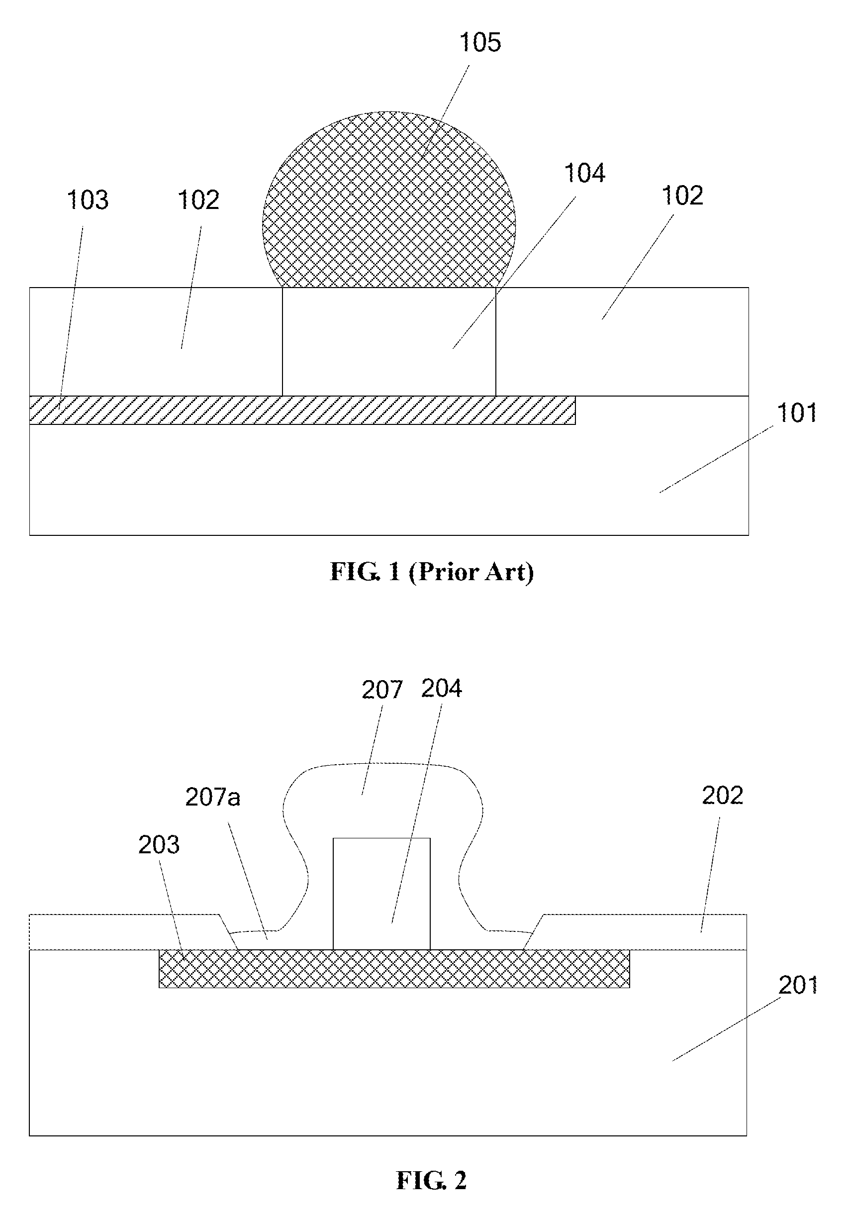
[0043]As described in the background, referring to FIG. 1, the solder ball 105 is disposed on the sub-ball metal electrode 104 and contacts with the upper surface of the sub-ball metal electrode 104. The contact area between the solder ball 105 and the sub-ball metal electrode 104 is relatively small, thus, the adhesion between the solder ball 105 and the sub-ball metal electrode 104 is relatively weak. Besides, when the solder ball 105 which is generally made of tin is formed on the upper surface of the sub-ball metal electrode 104 which is generally made of copper, the tin atoms and copper atoms may diffuse into each other, forming intermetallic compounds and cavities. The intermetallic compounds are fragile, which may affect the mechanical strength and service life of welded points.

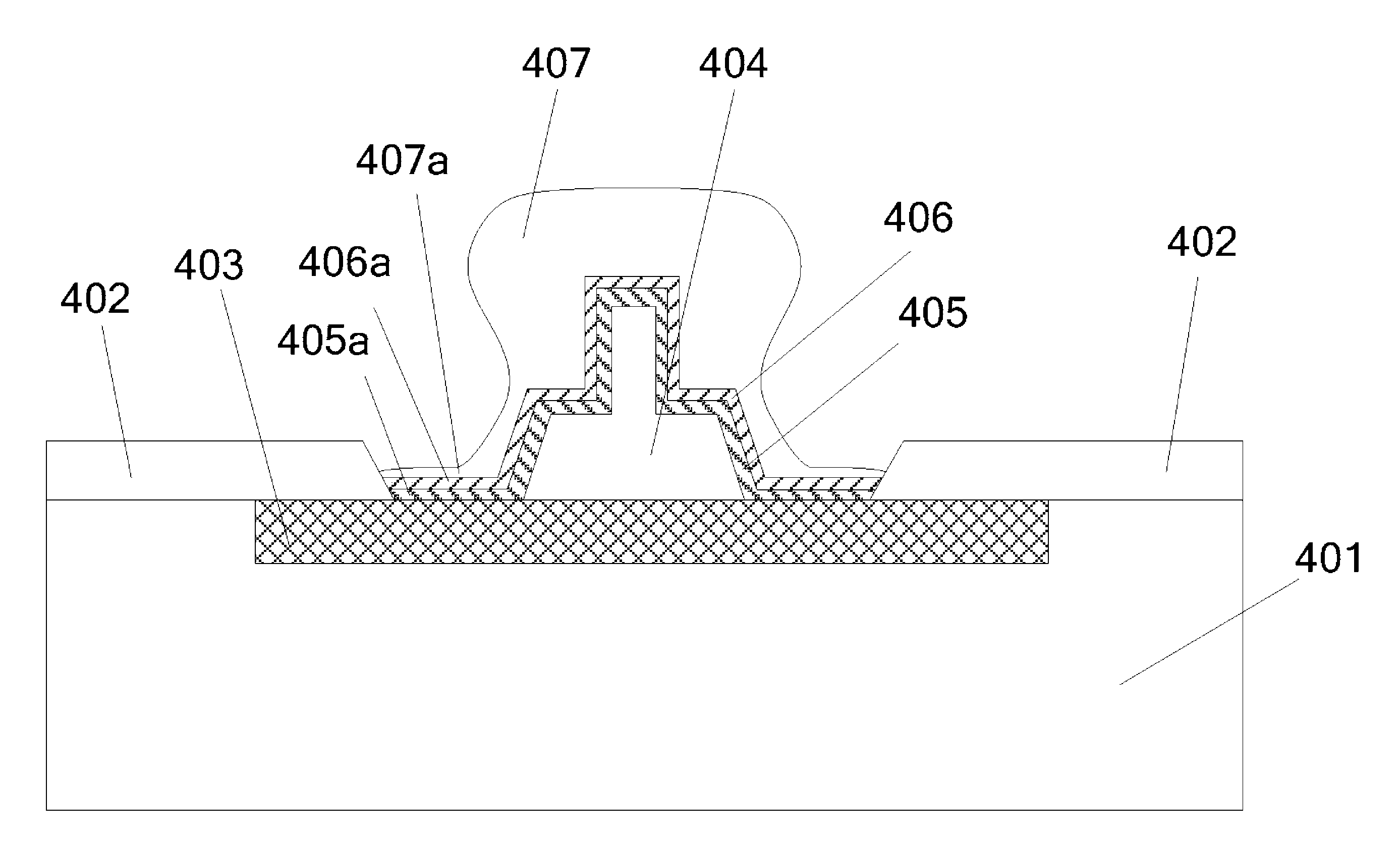
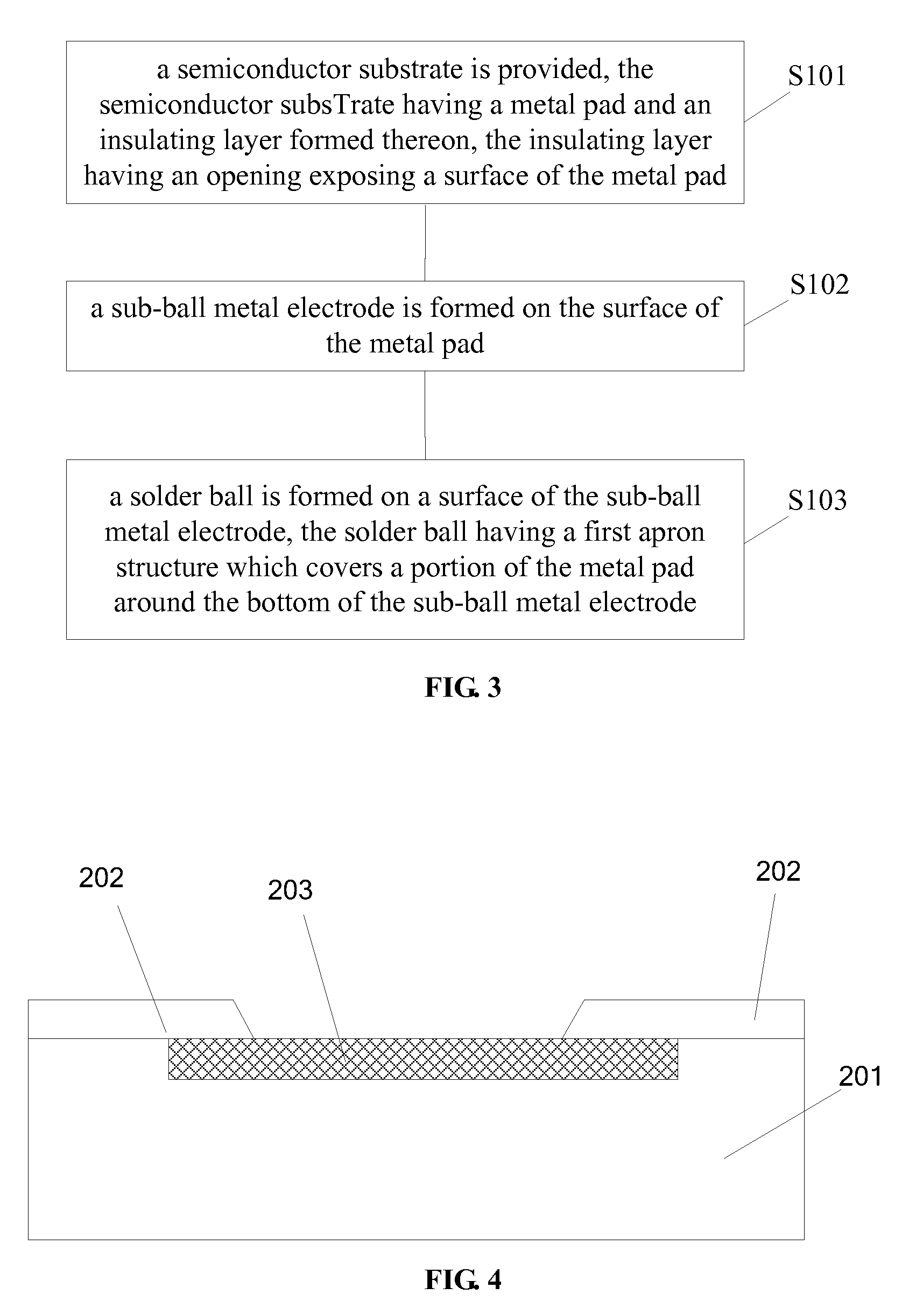
[0044]In embodiments of present disclosure, a chip package structure and a chip packaging method are provided. The chip package structure includes: a semiconductor substrate; a metal pad inside the sem...


PUM

PropertyMeasurementUnit
thicknessaaaaaaaaaa
thicknessaaaaaaaaaa
thicknessaaaaaaaaaa

Abstract

A chip packaging structure and packaging method. The packaging structure comprises: a semiconductor substrate; a metal pad provided inside the semiconductor substrate; an insulating layer provided on the semiconductor substrate, the insulating layer having an opening for exposing the metal pad; a sub-ball metal electrode provided on the metal pad; a solder ball provided on the surface of the sub-ball metal electrode, the solder ball having a first apron structure and the first apron structure covering partial metal pad on the periphery of the bottom of the under-ball metal electrode. The chip packaging structure of the present invention enhances the adhesion between the solder ball and the metal pad, and improves the reliability in chip packaging.

Description

CROSS-REFERENCE TO RELATED APPLICATIONS[0001]The present application is a Section 371 National Stage Application of International Application No. PCT / CN2013 / 086211, filed on Oct. 30, 2013, which claims priority to Chinese patent application No. 201210444502.4, filed on Nov. 8, 2012, and entitled “CHIP PACKAGE STRUCTURE”, and Chinese patent application No. 201210444530.6, filed on Nov. 8, 2012, and entitled “CHIP PACKAGING METHOD”, and the entire disclosures of which are incorporated herein by reference.FIELD OF THE DISCLOSURE[0002]The present disclosure generally relates to semiconductor technology, and more particularly, to a chip package structure and a chip packaging method.BACKGROUND OF THE DISCLOSURE[0003]In conventional techniques, Integrated Circuit (IC) chips are connected to external circuits by a wire bonding process. To meet the demand of small feature size of IC chips and the enlargement of a scale of ICs, the wire bonding process is less used. Wafer Level Chip Size Pack...

Claims


Application Information

Patent Timeline
Patent Type & Authority Patents(United States)
IPC IPC(8): H01L23/48H01L23/00B23K31/02H01L21/00H01L23/498
CPCH01L23/49816H01L24/11H01L24/16H01L24/29H01L24/81H01L24/83H01L24/13H01L24/06H01L2224/10125H01L2224/10145H01L2224/11013H01L2224/11825H01L2224/13008H01L2224/13084H01L2224/13099H01L2224/13553H01L2224/13561H01L2224/13599H01L2924/0105H01L2924/01028H01L2924/01047H01L2924/01079H01L2924/35H01L23/3192H01L24/02H01L24/05H01L2224/02331H01L2224/0401H01L2224/05548H01L2224/05624H01L2224/05639H01L2224/05644H01L2224/05647H01L2224/1132H01L2224/1134H01L2224/1145H01L2224/1146H01L2224/11462H01L2224/1147H01L2224/1182H01L2224/11849H01L2224/13007H01L2224/13017H01L2224/13018H01L2224/13024H01L2224/13076H01L2224/131H01L2224/13111H01L2224/13139H01L2224/13144H01L2224/13147H01L2224/13294H01L2224/133H01L2224/13311H01L2224/13541H01L2224/13562H01L2224/13582H01L2224/136H01L2224/13611H01L2224/13639H01L2224/13644H01L2224/13655H01L2224/13794H01L2224/138H01L2224/13811H01L2224/81191H01L2924/01039H01L2924/3651H01L2924/00014H01L2924/014H01L2924/00012
Inventor LIN, CHANG-MINGSHI, LEISHEN, HAIJUN
Owner NANTONG FUJITSU MICROELECTRONICS
Why Eureka
Try Eureka