Micro pick up array alignment encoder

an array alignment and encoder technology, applied in the direction of gripping heads, instruments, measurement devices, etc., can solve the problems of encoders not being integrated, encoders not being able to detect rotational or positional alignment of mems device components, and not being able to integrate encoders

Active Publication Date: 2016-03-29
APPLE INC
View PDF138 Cites 35 Cited by
  • Summary
  • Abstract
  • Description
  • Claims
  • Application Information

AI Technical Summary

Problems solved by technology

Integration and packaging issues are one of the main obstacles for the commercialization of micro devices such as radio frequency (RF) microelectromechanical systems (MEMS) microswitches, light-emitting diode (LED) display systems, and MEMS or quartz-based oscillators.
Traditionally, encoders have not been integrated within MEMS-scale devices, and where they have been used, the encoders do not detect rotational or positional alignment of the MEMS device components.

Method used


Image

  • Micro pick up array alignment encoder
  • Micro pick up array alignment encoder
  • Micro pick up array alignment encoder

Examples


Embodiment Construction

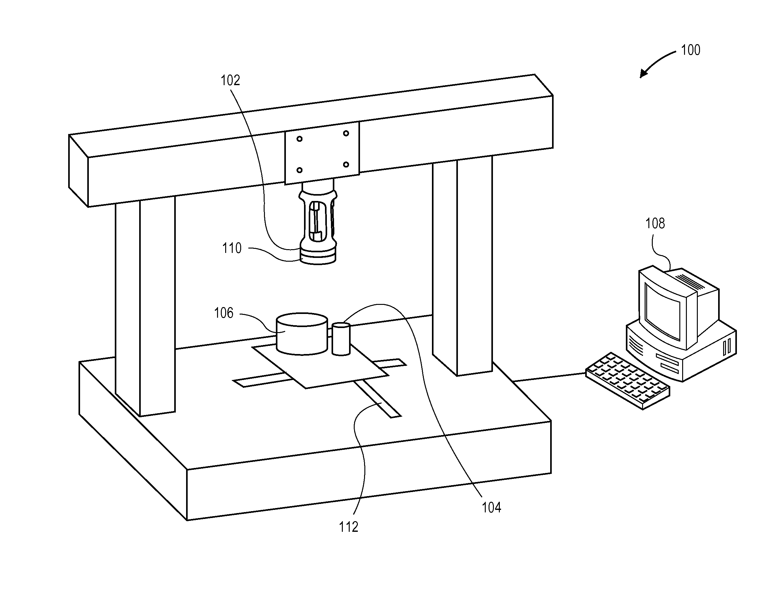
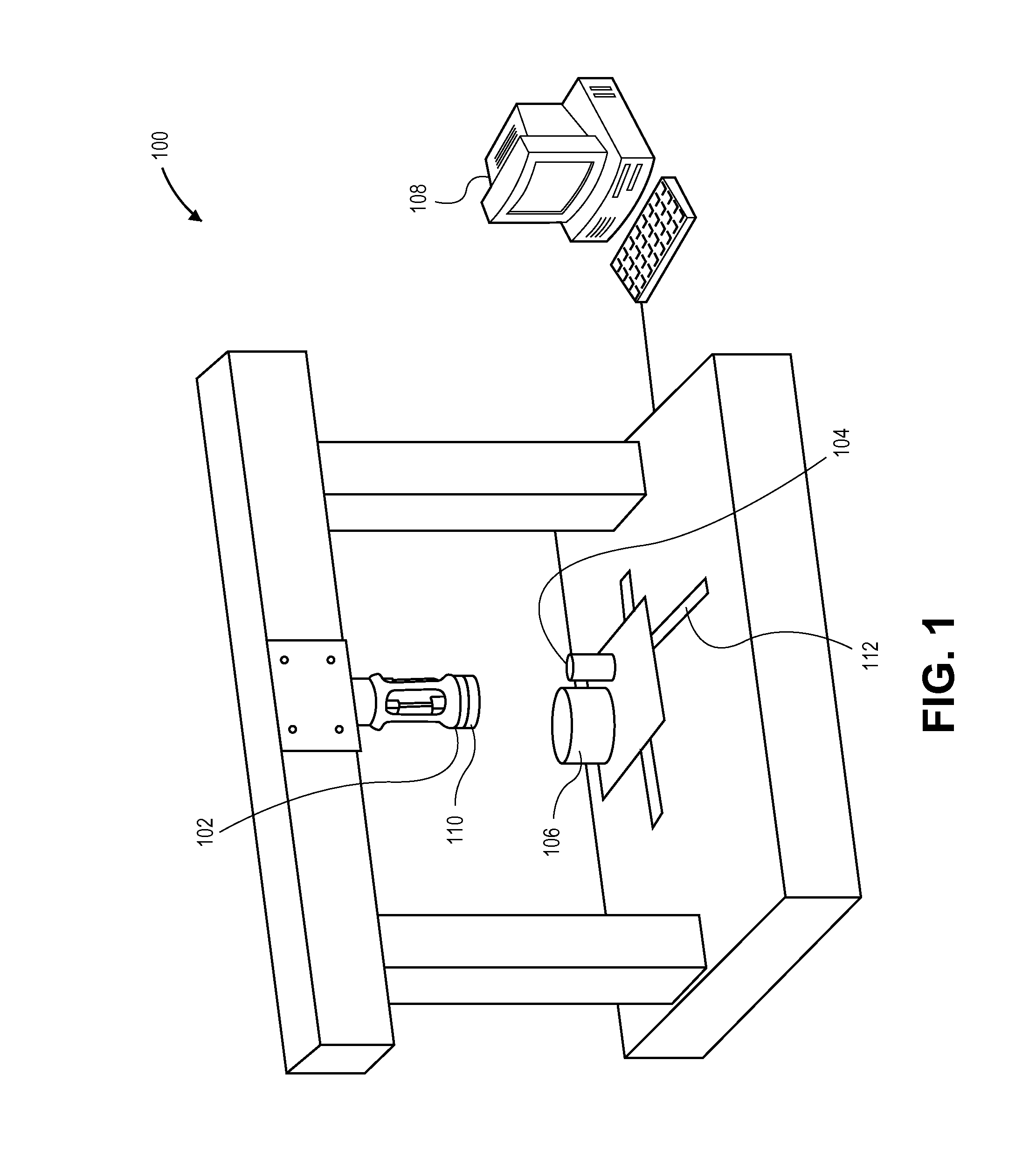
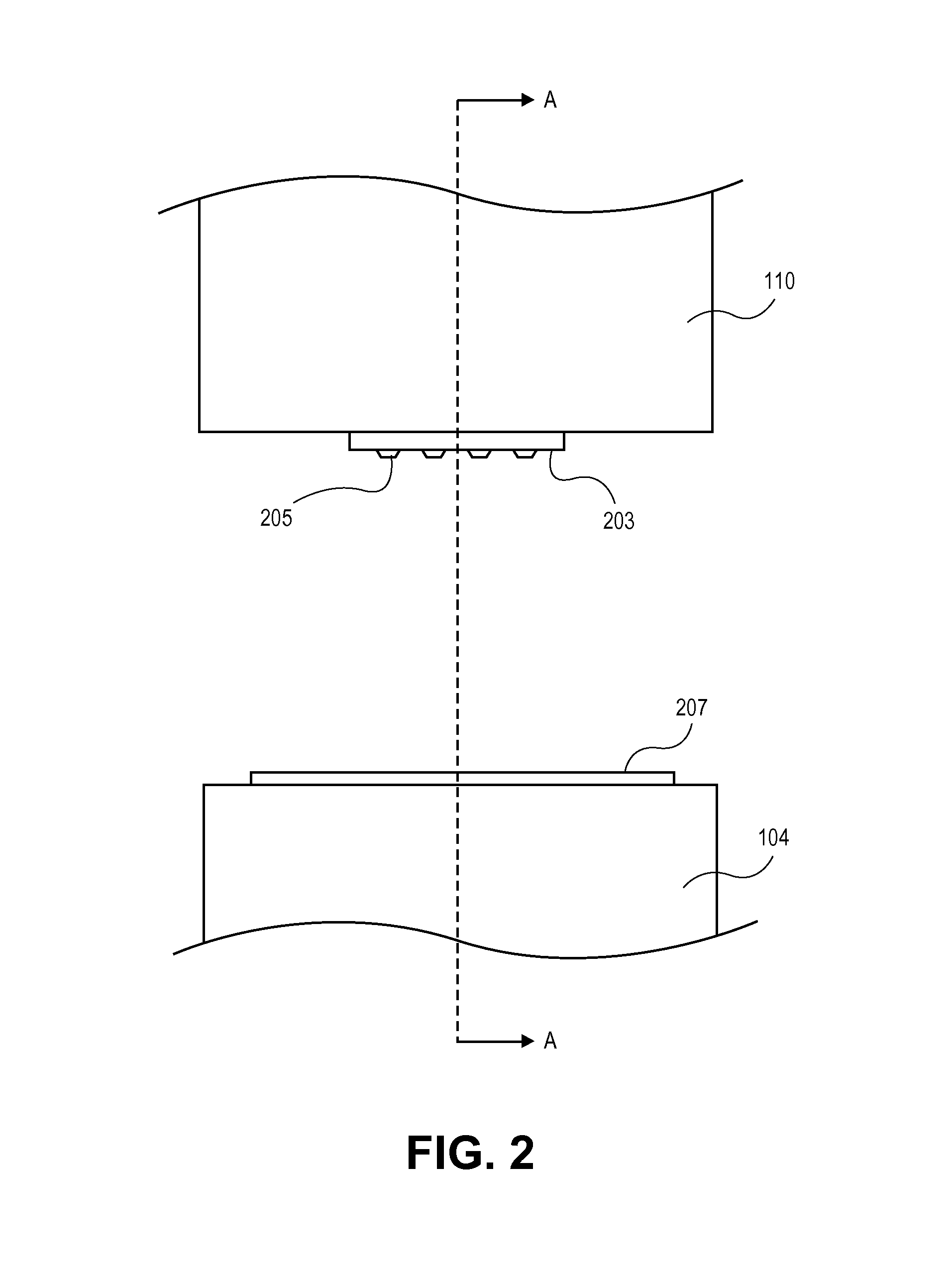
[0042]Embodiments of the present invention describe apparatuses and methods for alignment of transfer heads with a target substrate to facilitate transfer of micro devices. For example, the micro device or array of micro devices may be any of the micro LED device structures illustrated and described in related U.S. Patent Publications 2013 / 0126891 and 2013 / 0126081 and U.S. patent application Ser. Nos. 13 / 458,932 and 13 / 625,825. While some embodiments of the present invention are described with specific regard to micro LED devices, the embodiments of the invention are not so limited and certain embodiments may also be applicable to other micro devices such as diodes, transistors, integrated circuit (IC) chips, and MEMS.

[0043]In various embodiments, description is made with reference to the figures. However, certain embodiments may be practiced without one or more of these specific details, or in combination with other known methods and configurations. In the following description, nu...


PUM


Abstract

Micro pick up arrays and methods for transferring micro devices from a carrier substrate are disclosed. In an embodiment, a micro pick up array alignment encoder detects relative position between a micro pick up array having an encoder scale and a target substrate having a corresponding reference scale. In an embodiment, the micro pick up array alignment encoder facilitates alignment of the micro pick up array with the target substrate.

Description

BACKGROUND[0001]1. Field[0002]The present invention relates to alignment of transfer heads with a target substrate to facilitate transfer of micro devices.[0003]2. Background Information[0004]Integration and packaging issues are one of the main obstacles for the commercialization of micro devices such as radio frequency (RF) microelectromechanical systems (MEMS) microswitches, light-emitting diode (LED) display systems, and MEMS or quartz-based oscillators.[0005]Traditional technologies for transferring devices include, e.g., “transfer printing”, which involves using a transfer wafer to pick up an array of devices from a donor wafer. The array of devices are then bonded to a receiving wafer before removing the transfer wafer. Some transfer printing process variations have been developed to selectively bond and de-bond a device during the transfer process. In both traditional and variations of the transfer printing technologies, the transfer wafer is de-bonded from a device after bon...

Claims


Application Information

Patent Timeline
Patent Type & Authority Patents(United States)
IPC IPC(8): G01B11/00B25J15/00G01D5/347H01L21/68H01L21/67
CPCB25J15/0085G01D5/347H01L21/67144H01L21/681
Inventor BIBL, ANDREASPARKS, PAUL, ARGUS
Owner APPLE INC
Why Eureka
Try Eureka