

Packaged semiconductor device having leadframe features as pressure valves against delamination
- Summary
- Abstract
- Description
- Claims
- Application Information
AI Technical Summary
Benefits of technology
Problems solved by technology
Method used
Image

Examples
Embodiment Construction
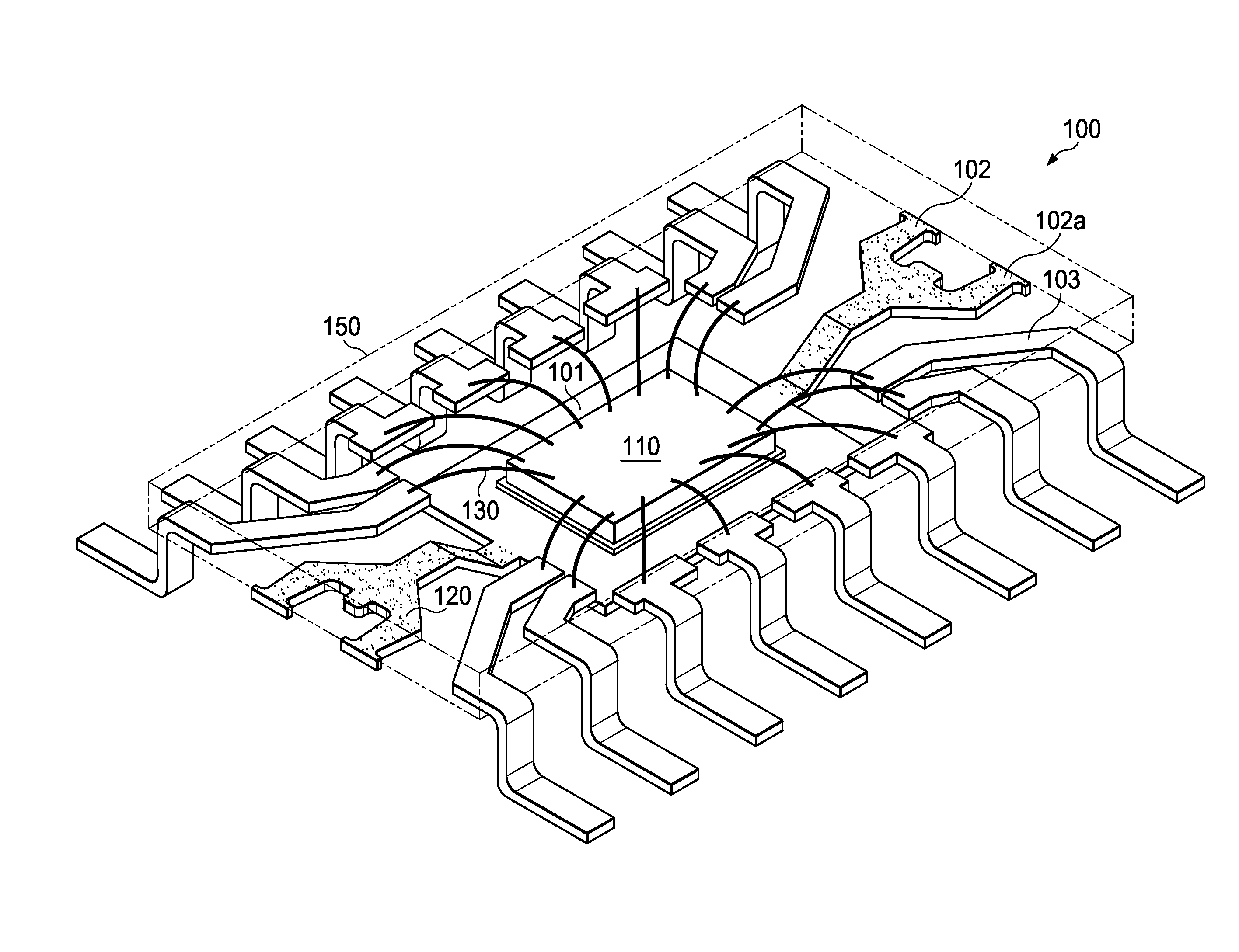
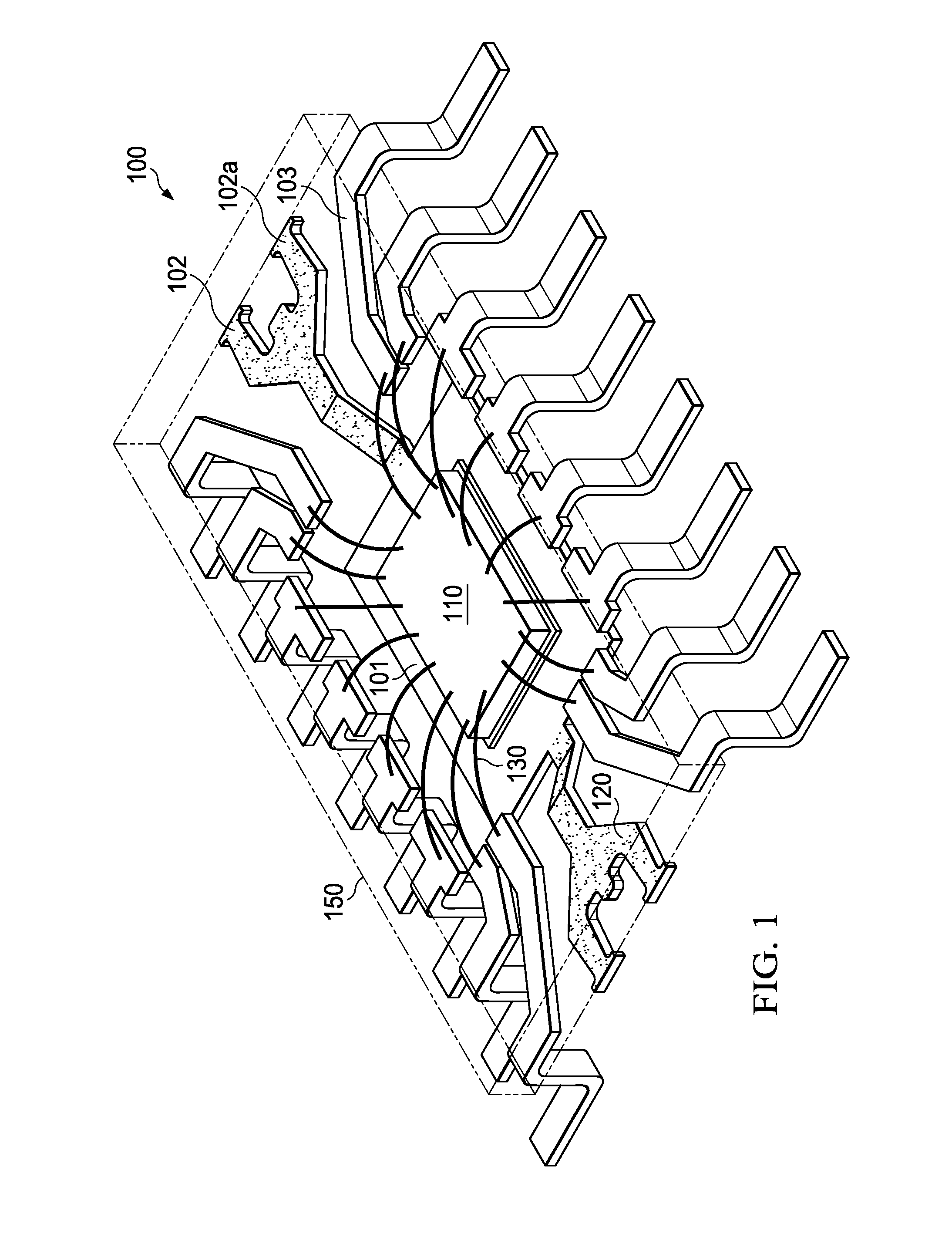
[0015]FIG. 1 illustrates an exemplary embodiment of the invention, a plastic packaged semiconductor device generally designated 100 with a metallic leadframe. The leadframe includes a pad 101 for assembling a semiconductor chip 110, tie bars 102 connecting pad 101 to the sidewall of the package, and a plurality of leads 103. It should be noted that herein the tie bars are referred to as straps. The chip terminals are connected to the leads 103 by bonding wires 130. In the example of FIG. 1, leads 103 are shaped as cantilevered leads; in other embodiments, the leads may have the shape of flat leads as used in Quad Flat No-Lead (QFN) devices or in Small Outline No-Lead (SON) devices. Along their longitudinal extension, straps 102 of the exemplary device in FIG. 1 include bendings and steps, since pad 101 and leads 103 are not in the same plane. In other devices, straps 102 are flat and planar, because pad 101 and leads 103 are in the same plane.
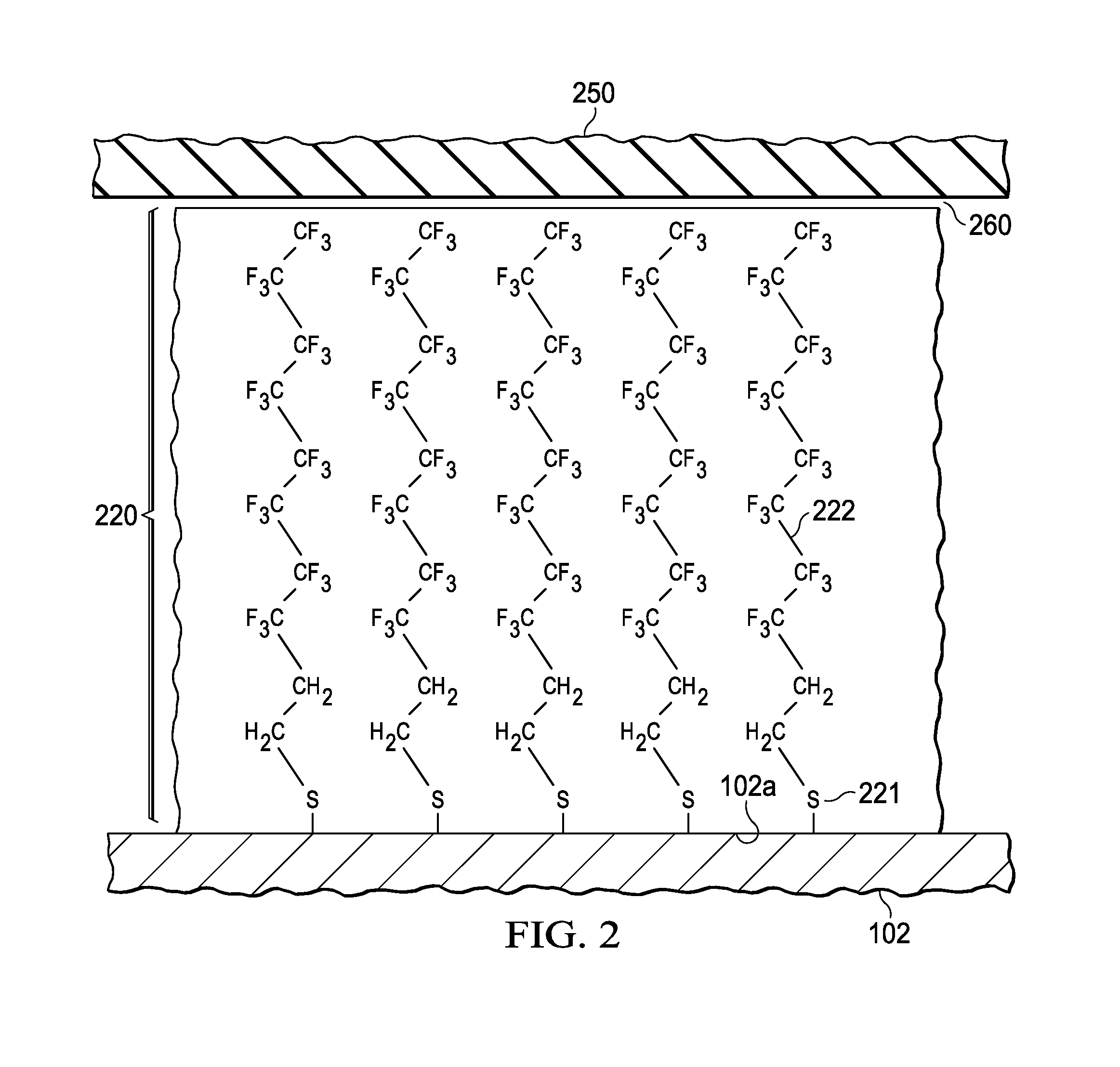
[0016]The leadframe surface onto which t...
PUM
 Abstract
Description
Claims
Application Information