Semiconductor structure having aluminum oxynitride film on germanium layer and method of fabricating the same

a technology of aluminum oxynitride and germanium layer, which is applied in the direction of basic electric elements, electrical apparatus, and semiconductor devices, can solve problems such as unstable germanium oxide (for example, geosub>2/sub>) and achieve the effect of suppressing the degradation of an interface condition

Active Publication Date: 2016-04-05
JAPAN SCI & TECH CORP
View PDF10 Cites 37 Cited by
  • Summary
  • Abstract
  • Description
  • Claims
  • Application Information

AI Technical Summary

Benefits of technology

[0019]According to the present invention, it is possible to suppress degradation of an interface condition between a germanium layer and an aluminum oxynitiride film.

Problems solved by technology

However, germanium oxide (for example, GeO2) is unstable.

Method used


Image

  • Semiconductor structure having aluminum oxynitride film on germanium layer and method of fabricating the same
  • Semiconductor structure having aluminum oxynitride film on germanium layer and method of fabricating the same
  • Semiconductor structure having aluminum oxynitride film on germanium layer and method of fabricating the same

Examples


embodiment 1

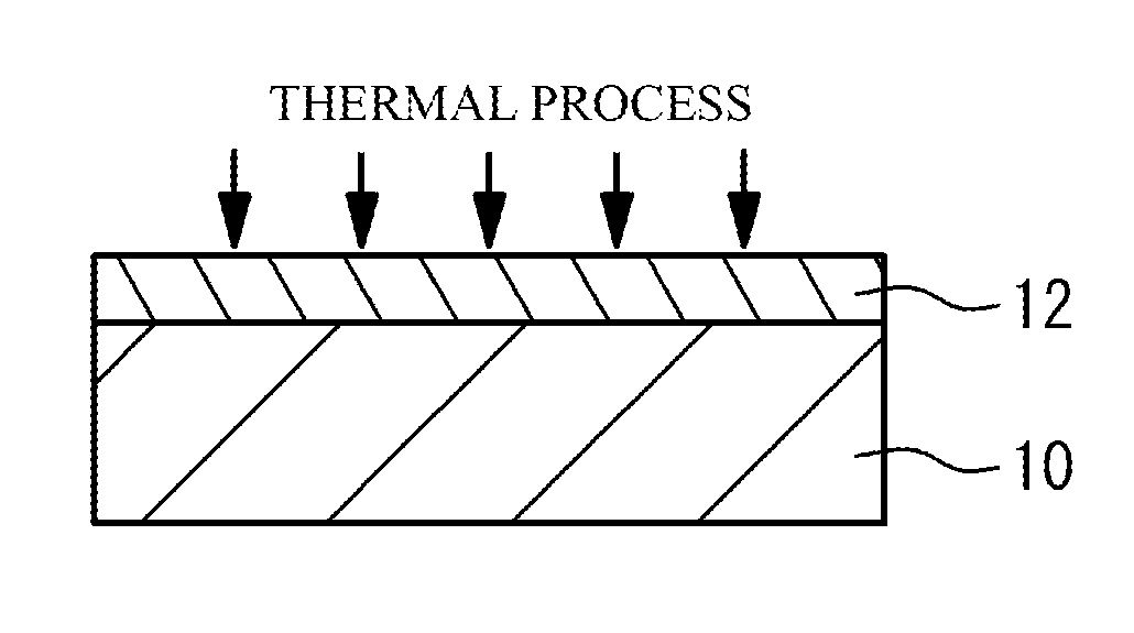
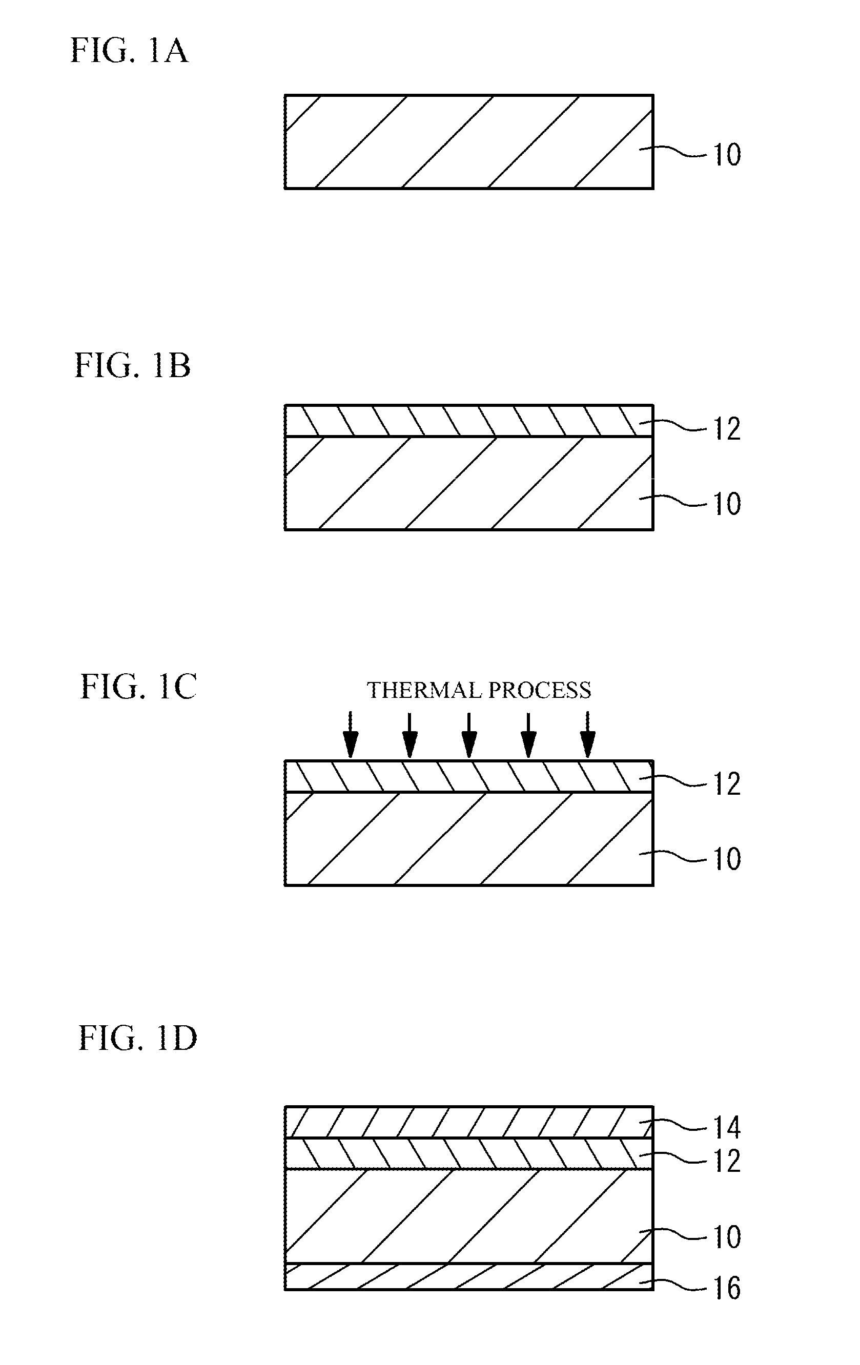
[0070]FIG. 11A to FIG. 11C illustrate a cross sectional view of the method of fabricating the semiconductor structure in accordance with an embodiment 1. As illustrated in FIG. 11A, a germanium layer 30 is prepared. The germanium layer 30 may be a single crystal germanium substrate or a germanium film formed on a substrate (for example, a silicon substrate). And, the germanium layer 30 may be highly-pure germanium or may include impurities. For example, the germanium layer 30 may be n-type or p-type germanium. Further, the germanium layer 30 may include silicon in an amount which achieves the effect of the above-mentioned experiments. At least, the composition ratio of the silicon is 10 atomic % or less of the whole. The main face of the germanium layer 30 may be a (111) face or the like. However, the main face may be another face such as a (110) face or a (100) face.

[0071]As illustrated in FIG. 11B, an aluminum oxynitride film 32 is formed on the germanium layer 30. The aluminum ox...


PUM

PropertyMeasurementUnit
frequencyaaaaaaaaaa
pressureaaaaaaaaaa
pressureaaaaaaaaaa

Abstract

A semiconductor structure includes: a germanium layer 30; and an aluminum oxynitride film 32 that is formed on the germanium layer, wherein: an EOT of the aluminum oxynitride film is 2 nm or less; Cit / Cacc is 0.4 or less; on a presumption that Au acting as a metal film is formed on the aluminum oxynitride film, the Cit is a capacitance value between the germanium layer and the metal film at a frequency of 1 MHz in a case where a voltage of the metal film with respect to the germanium layer is applied to an inversion region side by 0.5 V; and the Cacc is a capacitance value between the germanium layer and the metal film in an accumulation region.

Description

CROSS REFERENCE TO RELATED APPLICATIONS[0001]The present application is a Continuation of International Patent Application No. PCT / JP2013 / 056678, filed on Mar. 11, 2013, which claims priority to and the benefit of Japanese Patent Application No. 2012-185276, filed on Aug. 24, 2012, the entire contents of each of which are incorporated by reference herein.TECHNICAL FIELD[0002]The present invention relates to a semiconductor structure having an aluminum oxynitride film on a germanium layer and a method of fabricating the semiconductor structure.BACKGROUND ART[0003]Germanium (Ge) is a semiconductor that has better electrical properties than silicon (Si). However, germanium oxide (for example, GeO2) is unstable. Therefore, the germanium oxide is rarely used for a semiconductor material forming a MOSFET (Metal Oxide Semiconductor Field Effect Transistor).[0004]For example, non-patent documents 1 and 2 disclose that an aluminum nitride (AlN) film is used as a part of a gate insulating fil...

Claims


Application Information

Patent Timeline
Patent Type & Authority Patents(United States)
IPC IPC(8): H01L27/01H01L29/16H01L21/3105H01L29/51H01L29/78H01L21/02H01L21/28
CPCH01L29/512H01L29/513H01L29/518H01L29/78H01L29/517H01L21/02337H01L21/28255H01L21/3105H01L29/16H01L21/02178H01L21/02266H01L21/02318
Inventor TORIUMI, AKIRATABATA, TOSHIYUKI
Owner JAPAN SCI & TECH CORP
Why Eureka
Try Eureka