

Transition between a microstrip protruding into an end of a closed waveguide having stepped sidewalls
a closed waveguide and microstrip technology, applied in the direction of waveguide type devices, coupling devices, basic electric elements, etc., can solve the problems of increasing the difficulty of using this technology with increasing frequencies and/or bandwidth, requiring two waveguide pieces, and high loss of e-probe transition, etc., to achieve strong coupling, increase field coupling, and build up field strength
- Summary
- Abstract
- Description
- Claims
- Application Information
AI Technical Summary
Benefits of technology
Problems solved by technology
Method used
Image

Examples
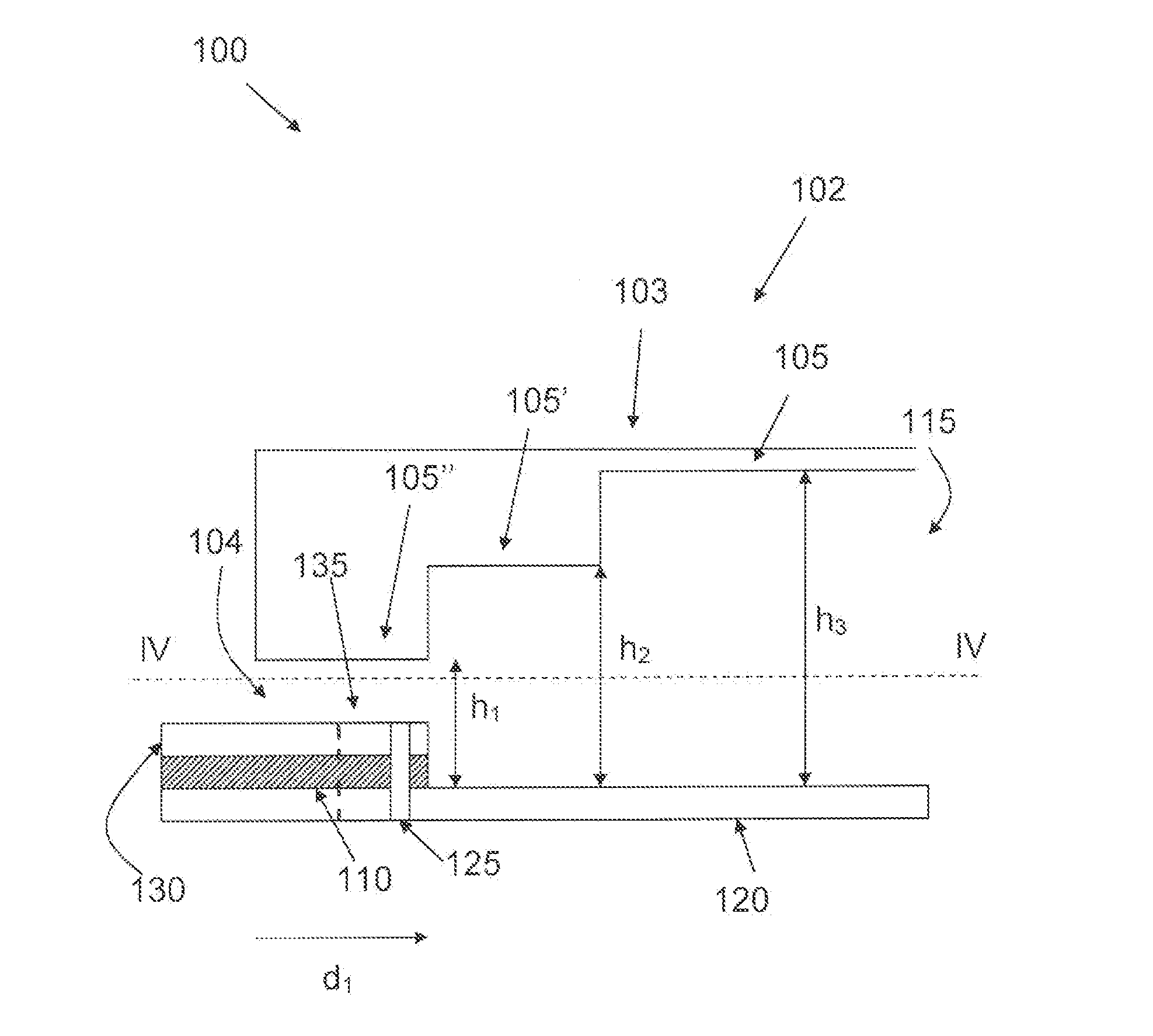
embodiment 100
[0048]FIG. 4 shows the embodiment 100 of FIG. 1 in an open view along the line IV-IV of FIG. 1, i.e. in a “top view” with the ceiling 105 of the closed waveguide 102 removed. In this view, the patch 135, and the other part of the microstrip conductor 130, which connects to the patch 135 can be seen more clearly. Here, it can be see more clearly how the microstrip conductor 130 connects to the conducting patch 135. Another way of looking at this is to say that the microstrip conductor 130 and the conducting patch 135 are part of one and the same conducting (metal) layer or “body”, and that there is a seamless transition in this body from microstrip conductor 130 to the conducting patch 135. In addition, the different widths w1 of the microstrip conductor 130 and w3 of the conducting patch 135 can also be seen here, as well as the length L1 of the conducting patch 135. It should be pointed out that although the conducting patch 135 is shown and described here as being rectangular, the...
embodiment 300
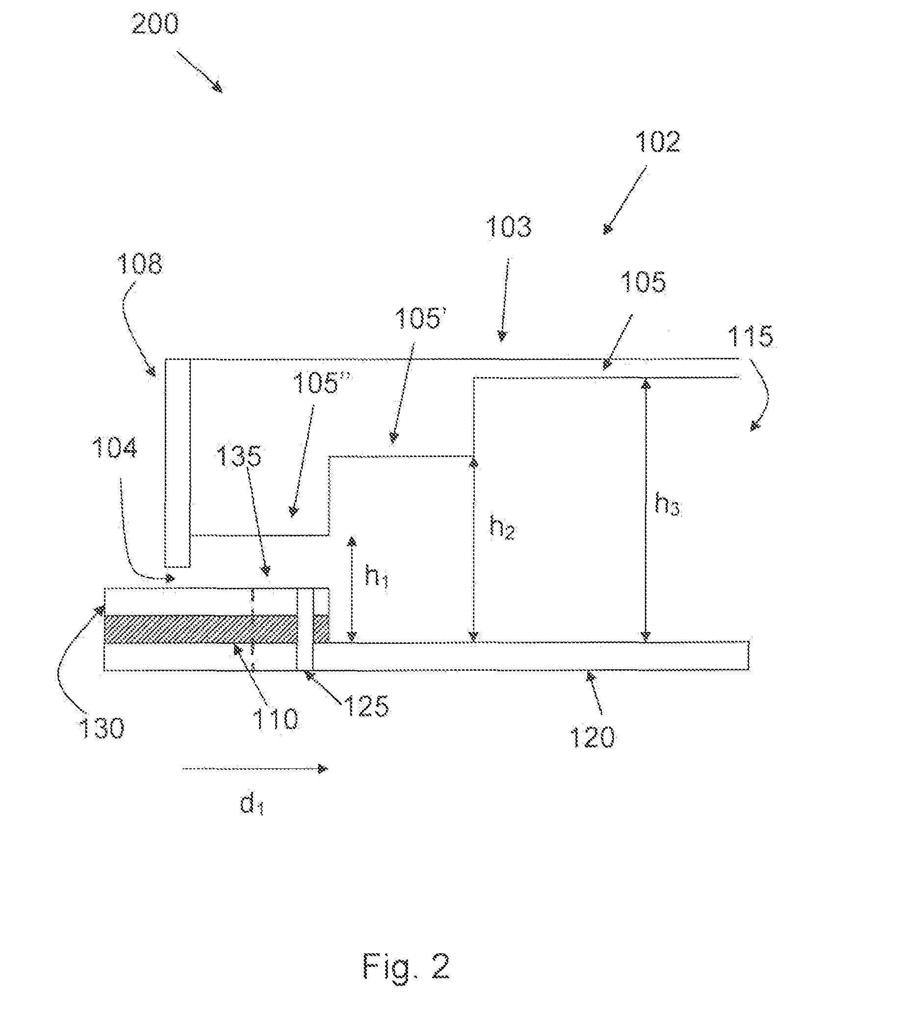
[0050]Thus, as shown in FIG. 5, in the embodiment 300, the dielectric layer 110 extends beyond the distance d1, into the closed waveguide 102 on the first main surface 120. In one embodiment, which is shown in FIG. 5, the dielectric layer 110 protrudes into the closed waveguide 102 beyond the conducting patch 135, and is covered by an upper layer 140 of a conducting material which can be separated from the conducting patch 135 by a distance d2. A distance d3 is also show in FIG. 5, which is an example of how far the upper layer 140 of a conducting material extends into the closed waveguide 102. FIG. 5 also shows a second via connection 129.
[0051]The different heights h1, h2 and h3 of the side walls 115, 116 (not shown), are in FIG. 5 shown as extending only from the upper layer 140 of a conducting material. Although this is correct, it should however be pointed out that the proportions in the drawings are not to scale, but are greatly magnified in some cases: for example, the thickn...
PUM
 Abstract
Description
Claims
Application Information