
Methods for forming FinFETS having a capping layer for reducing punch through leakage

a fin and capping layer technology, applied in the direction of transistors, electrical apparatus, semiconductor devices, etc., can solve the problems of increasing static power consumption, increasing variability, and affecting the efficiency of submicron devices, so as to reduce the leakage path from source to drain, increase positive charge, and increase negative charge

Active Publication Date: 2016-04-12
ALSEPHINA INNOVATIONS INC
View PDF4 Cites 18 Cited by
  • Summary
  • Abstract
  • Description
  • Claims
  • Application Information

AI Technical Summary

Benefits of technology

The patent is about a method to reduce punch-through leakage in semiconductor devices. It involves providing a semiconductor substrate with a plurality of fins and capping layers over the fins. The capping layers can provide increased negative or positive charges to reduce leakage. The method also includes removing portions of the capping layers and isolation fill to expose the upper surface portions of the fins. The semiconductor structure produced using this method has improved performance and reliability.

Problems solved by technology

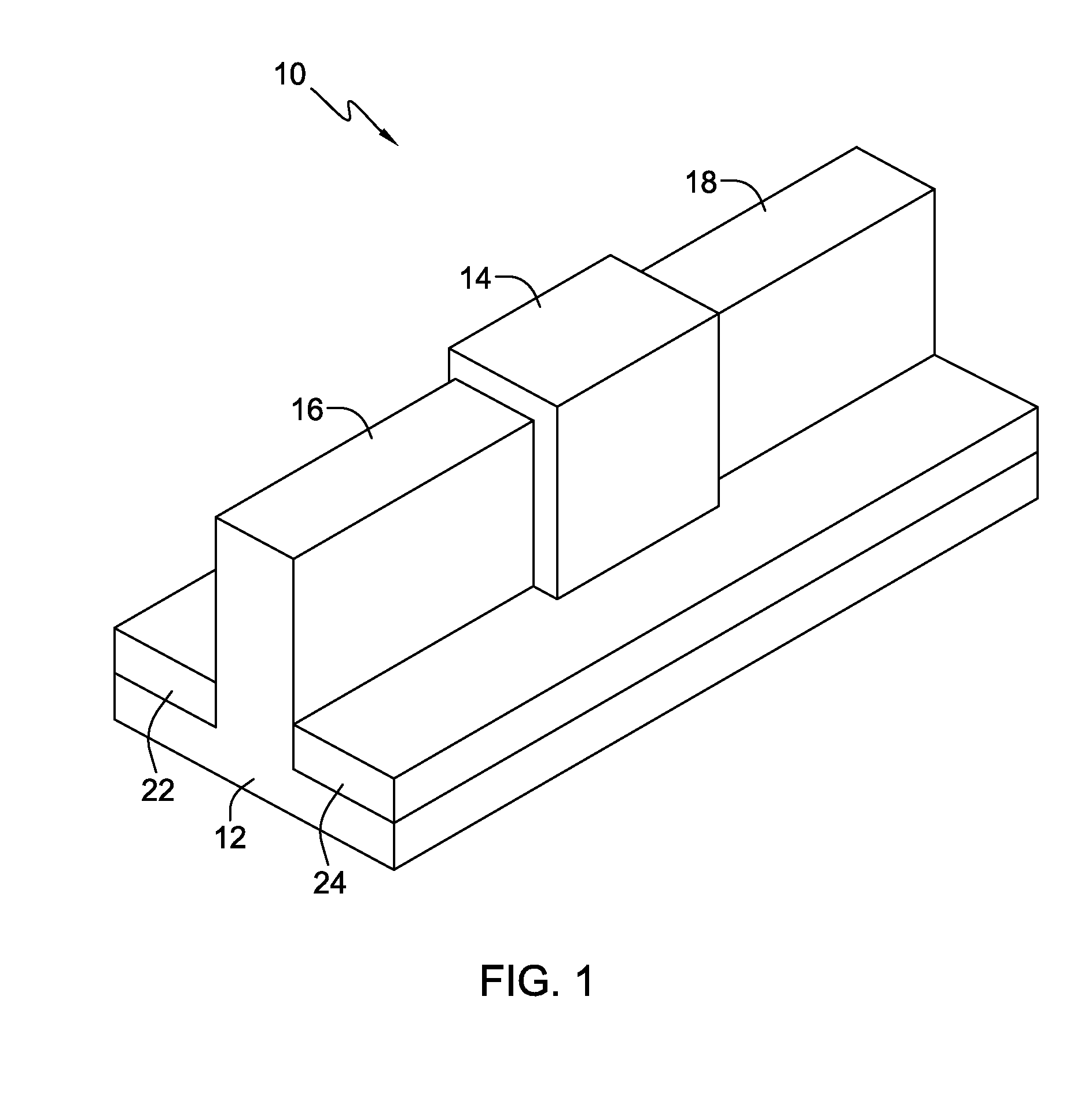
However, a problem with bulk short channel FinFET devices, is that a leakage path from source to drain exists through a portion of the fin not covered by the gate, but lies below the channel.
The leakage of current from source to drain through the lower (un-gated) part of the fin that is not covered by the gate, commonly known as punch-through leakage, causes an increase of static power consumption which is undesirable in modern submicron devices.
However, the impurities doped by the punch-through-stopper (PTS) implantation may diffuse into the channel region, increasing the variability due to random dopant fluctuation (RDF) and lowering the carrier mobility of the channel region.

Method used


Image

  • Methods for forming FinFETS having a capping layer for reducing punch through leakage
  • Methods for forming FinFETS having a capping layer for reducing punch through leakage
  • Methods for forming FinFETS having a capping layer for reducing punch through leakage

Examples


Embodiment Construction

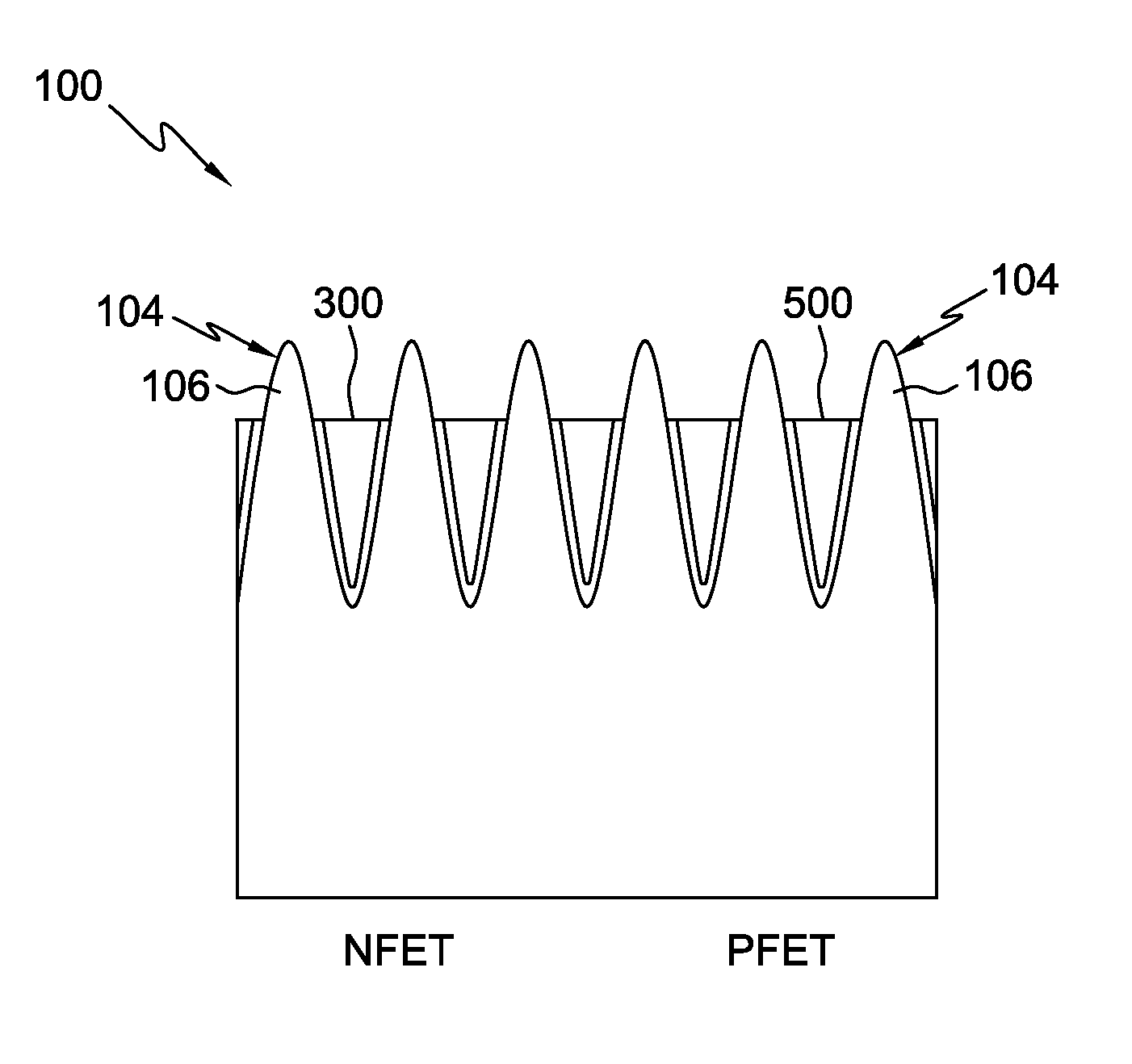
[0018]Aspects of the present disclosure and certain features, advantages, and details thereof, are explained more fully below with reference to the non-limiting embodiments illustrated in the accompanying drawings. Descriptions of well-known materials, fabrication tools, processing techniques, etc., are omitted so as to not unnecessarily obscure the disclosure in detail. It should be understood, however, that the detailed description and the specific examples, while indicating embodiments of the present disclosure, are given by way of illustration only, and are not by way of limitation. Various substitutions, modifications, additions and / or arrangements within the spirit and / or scope of the underlying concepts will be apparent to those skilled in the art from this disclosure. Reference is made below to the drawings, which are not drawn to scale for ease of understanding, wherein the same reference numbers used throughout different figures designate the same or similar components.

[00...


PUM


Abstract

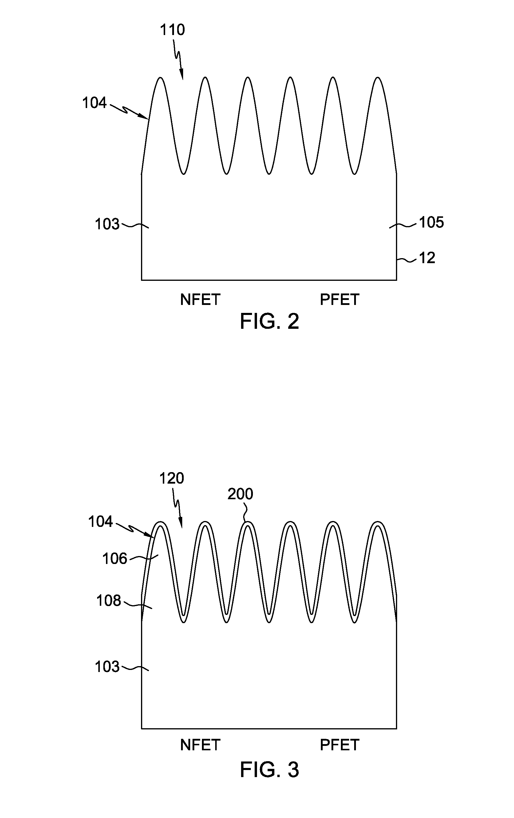
A method for forming FinFETs having a capping layer for reducing punch through leakage includes providing an intermediate semiconductor structure having a semiconductor substrate and a fin disposed on the semiconductor substrate. A capping layer is disposed over the fin, and an isolation fill is disposed over the capping layer. A portion of the isolation fill and the capping layer is removed to expose an upper surface portion of the fin. Tapping layer and a lower portion of the fin define an interface dipole layer barrier, a portion of the capping layer operable to provide an increased negative charge or an increased positive charge adjacent to the fin, to reduce punch-through leakage compared to a fin without the capping layer.

Description

TECHNICAL FIELD[0001]The present disclosure relates generally to conductive circuits and methods of forming conductive circuits, and more particularly, a capping treatment of a fin in the fabrication of a FinFET structure to reduce punch-through leakage.BACKGROUND OF THE DISCLOSURE[0002]Fin field-effect transistors (FinFET) devices have been developed to replace conventional planar bulk MOSFETs in advanced CMOS technology due to their improved short-channel effect immunity and Ion / Ioff ratio. However, a problem with bulk short channel FinFET devices, is that a leakage path from source to drain exists through a portion of the fin not covered by the gate, but lies below the channel. The leakage of current from source to drain through the lower (un-gated) part of the fin that is not covered by the gate, commonly known as punch-through leakage, causes an increase of static power consumption which is undesirable in modern submicron devices.[0003]In one solution, punch-through leakage in ...

Claims


Application Information

Patent Timeline
Patent Type & Authority Patents(United States)
IPC IPC(8): H01L21/336H01L21/8234H01L27/088
CPCH01L21/823437H01L21/823431H01L27/0886H01L21/823821H01L21/823878H01L27/0924H01L21/845H01L29/7854H01L27/1211H01L29/66795H01L29/0653H01L29/1083H01L29/785
Inventor KIM, HOONSUNG, MIN GYU
Owner ALSEPHINA INNOVATIONS INC
Learn More