Nanowire device with improved epitaxy

a nanowire and epitaxy technology, applied in the field of stacking nanowire devices, can solve problems such as design challenges and voltage leakage across the gate region, and achieve the effect of improving epitaxy

Inactive Publication Date: 2016-04-19
IBM CORP
View PDF10 Cites 21 Cited by
  • Summary
  • Abstract
  • Description
  • Claims
  • Application Information

AI Technical Summary

Benefits of technology

[0004]As disclosed herein, a method for fabricating a nanowire device with improved epitaxy, includes forming a nanowire stack on a substrate, the nanowire stack having one or more sacrificial layers, where the substrate includes a bulk substrate, an oxide layer, and an extremely thin silicon-on-insulator (ETSOI) layer, removing the sacrificial layers, depositing and patterning a gate material over the nanowire stack, the gate material having sidewalls, covering the sidewalls of the gate material with a spacer layer, and epitaxially growing an in-situ doped layer comprised of doped silicon from the ETSOI layer. The ETSOI may have a (100) crystallographic orientation. The nanowire stack and spacer layer may

Problems solved by technology

While integrated circuit manufacturers have been successful in exponentially decreasing the size of the components on the integrated circuit, design challenges have surfaced along t

Method used


Image

  • Nanowire device with improved epitaxy
  • Nanowire device with improved epitaxy
  • Nanowire device with improved epitaxy

Examples


Embodiment Construction

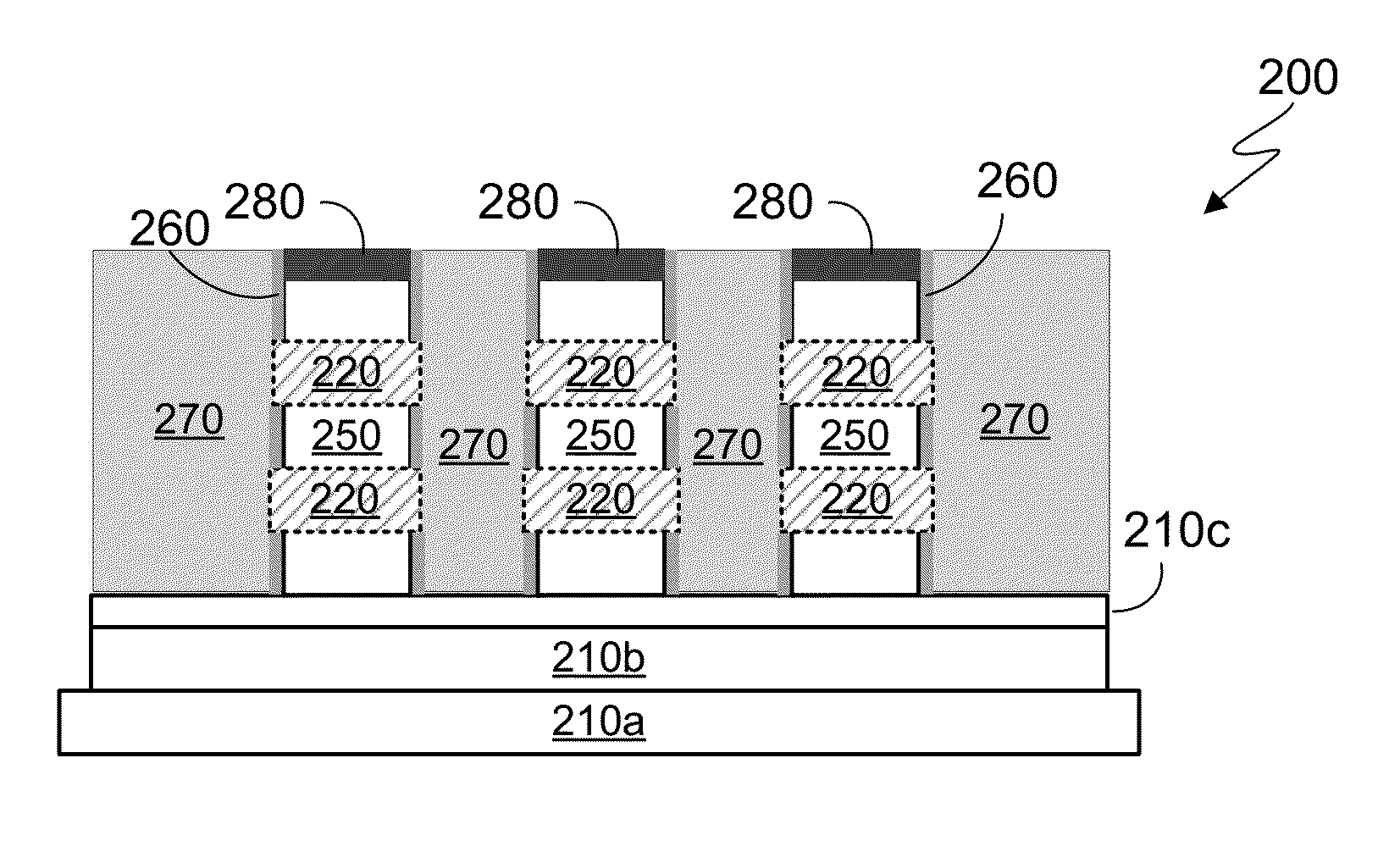
[0008]Rapid advancements in chip-containing technologies have led to a need to decrease the size of the semiconductor devices, including transistors. However, the source / drain regions of the semiconductor devices may be compromised when the size of the circuit is decreased.

[0009]The disclosed embodiments provide a method and device for improved epitaxial source / drain regions for a semiconductor device. To create a more effective source / drain region, a large surface area is needed. Growing a source / drain region epitaxially from the substrate enables a greater surface area to be utilized than in past technologies. Additionally, nanowires may be made smaller because the surface of the wire is not needed for epitaxial growth.

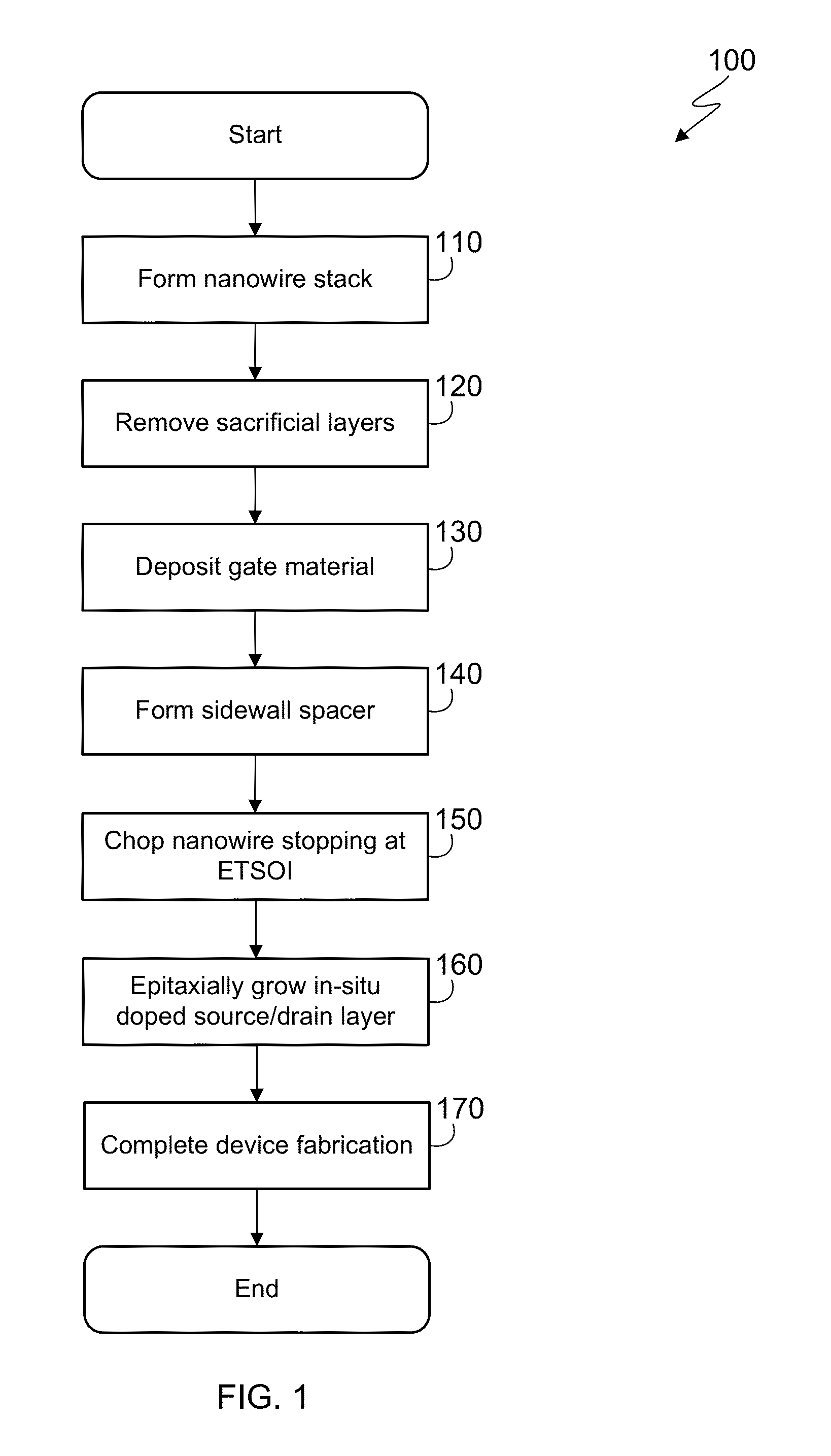
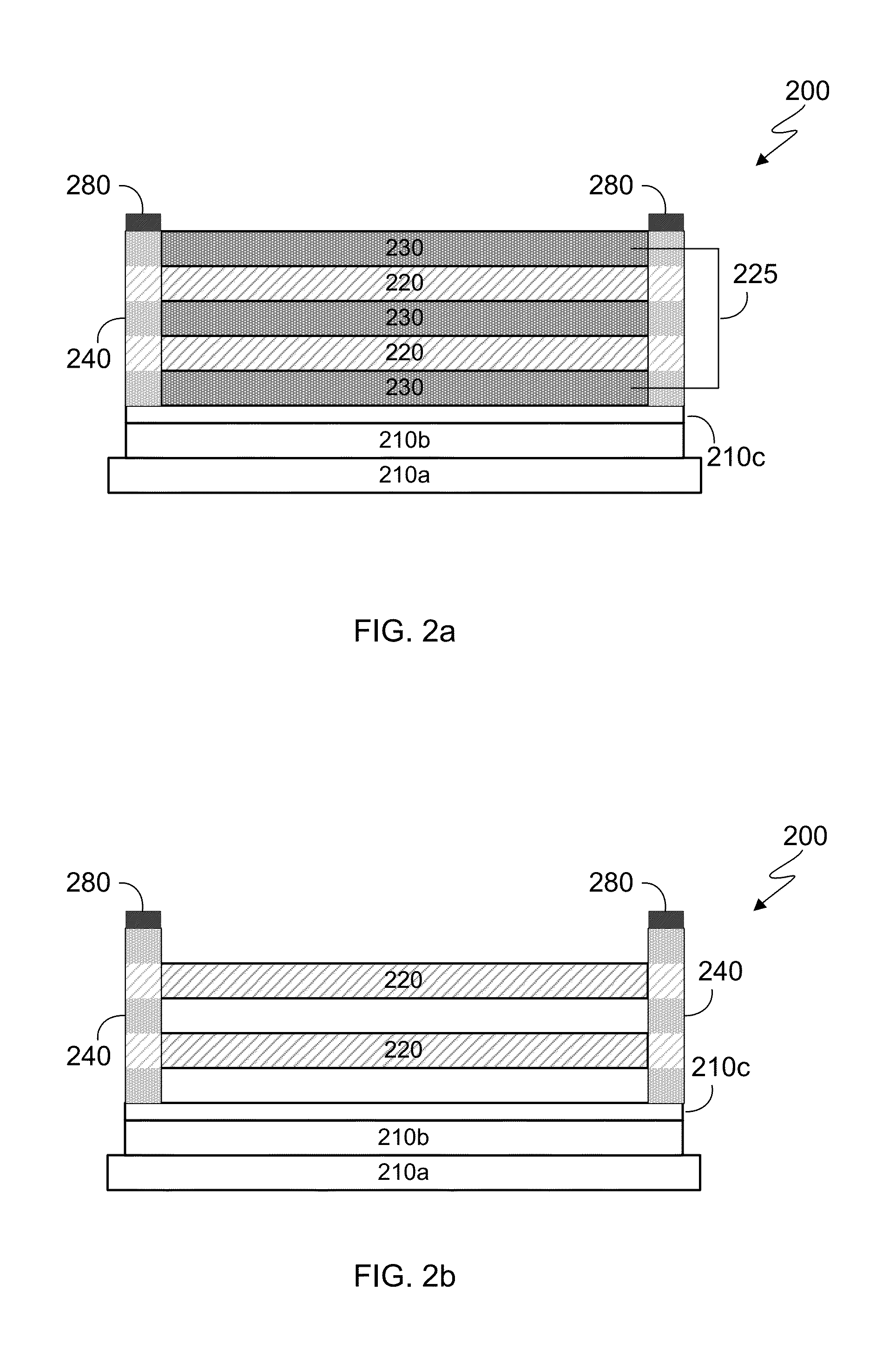
[0010]FIG. 1 is a flowchart depicting one embodiment of a nanowire device fabrication method 100. As depicted, the nanowire device fabrication method 100 includes forming (110) a nanowire stack, removing (120) the sacrificial layers from the nanowire stack, depositi...


PUM


Abstract

As disclosed herein, a method for fabricating a nanowire device with improved epitaxy, includes forming a nanowire stack on a substrate, the nanowire stack having one or more sacrificial layers, where the substrate includes a bulk substrate, an oxide layer, and an extremely thin silicon (ETSOI) layer, removing the sacrificial layers, depositing and patterning a gate material over the nanowire stack, the gate material having sidewalls, covering the sidewalls of the gate material with a spacer layer, and epitaxially growing an in-situ doped layer comprised of doped silicon from the ETSOI layer. The ETSOI may have a (100) crystallographic orientation. A pFET source/drain may be epitaxially grown by including an in-situ doped layer of boron doped SiGe. An nFET source/drain may be epitaxially grown by including an in-situ doped layer of phosphorus doped Si:C. A device corresponding to the method is also disclosed herein.

Description

BACKGROUND OF THE INVENTION[0001]The present invention relates generally to the field of semiconductor devices, and more particularly to stacked nanowire devices.[0002]There is a growing demand in the electronics market for smaller devices. To satisfy the wants and needs of consumers, the individual components of integrated circuits must decrease in size. While integrated circuit manufacturers have been successful in exponentially decreasing the size of the components on the integrated circuit, design challenges have surfaced along the way.[0003]Transistors are an integral element of the integrated circuit. Reducing the size of the transistor also reduces the size of the integrated circuit. However, as the transistor—and therefore the individual elements of the transistor—has decreased in size, problems have developed with voltage leaking across the gate region. To meet the needs of the electronic industry, integrated circuit designers must finds ways to minimize voltage leaks.SUMMA...

Claims


Application Information

Patent Timeline
IPC IPC(8): H01L29/16H01L29/06H01L29/66H01L29/04H01L21/02H01L29/167H01L29/786
CPCH01L29/0673H01L29/66742H01L29/0649H01L29/045H01L21/02422H01L21/02529H01L21/02532H01L21/02433H01L29/167H01L21/0257H01L29/78696H01L29/42392H01L29/66439H01L29/66772H01L29/775H01L29/78654H01L29/78684
Inventor CHENG, KANGGUOHASHEMI, POUYAKHAKIFIROOZ, ALIREZNICEK, ALEXANDER
Owner IBM CORP
Why Eureka
Try Eureka