
Method for sputter targets for electrolyte films

a technology of electrolyte film and sputter target, which is applied in the direction of sustainable manufacturing/processing, non-aqueous electrolyte cells, cell components, etc., can solve the problems of affecting the film growth on the substrate, the use of ceramic insulating sputter target and the rf sputter method may be undesirable, and the sputter process is affected. , to achieve the effect of less frequent maintenance schedule, thermal gradient, and high thermal conductivity ratio

Active Publication Date: 2016-05-10
SAPURAST RES
View PDF946 Cites 36 Cited by
  • Summary
  • Abstract
  • Description
  • Claims
  • Application Information

AI Technical Summary

Benefits of technology

[0021]A further aspect of an embodiment of the invention involves the generally higher thermal conductivity of metallic targets compared to their ceramic counterparts. This allows for the use of thicker metallic sputter targets, because for a given sputter target thickness the target cooling from the cooled target backing plate through the entire bulk of the sputter target is more efficient for metallic targets while additionally their thermal gradients are typically much smaller. Associated with the beneficial option of using thicker metallic targets is a less frequent maintenance schedule, reduced down-time of the production equipment, and thus lower fabrication costs of the thin film electrochemical storage and conversion devices because thicker sputter targets can be operated for longer periods before they have to be replaced. A compromise between target thickness and magnetron action at the sputter target surface may need to be made in order to optimize the performance of the production sputter equipment.

Problems solved by technology

However, both the use of the ceramic insulating sputter target and the RF sputter method may be undesirable due to their associated high costs, limitations in deposition area and rate, and hardware sophistication and challenges.
Electric arcing could be either so severe that electronics in the power supply connected to the sputter target may not prevent this event from occurring, which detrimentally affects the film growth on the substrate, or the sputter process could be interrupted too frequently by the preventive electronics of the power supply that a sputter deposition may not take place.
Unfortunately, the entire RF electronics around a sputter target are fairly expensive as well as require the vacuum deposition chamber to be RF compatible.
The design and build of new, large vacuum deposition chambers takes substantial amounts of time and money because these chambers are not anticipated to be built and sold in large numbers.
Another issue in RF sputtering is that, for deposition of oxide dielectric films, ceramic targets are typically formed of multiple smaller tiles due to limitations in fabricating large area ceramic sputter targets in thicknesses (e.g. ¼ inch) that are appropriate for use in sputter processes.
Further, the reactors required for RF sputtering tend to be rather complicated.
In particular, the engineering of low capacitance efficient RF power distribution to the sputter cathode is difficult in RF systems.
Typically, it has been difficult to fabricate large area, insulating, ceramic sputter targets because their constituent tile size, singly-tiled or multi-tiled, is limited by today's available ceramic processing methods (cold pressing plus subsequent sintering or, instead, hot pressing of appropriate starting powders) in light of the performance requirements for ceramic sputter target tiles when sputtered under the thermal stresses of high rate sputter deposition.
However, owing to the inherent brittleness of ceramic tiles and their limited, practical thickness when to be used in magnetron sputter targets (typical thickness is about ½ to ¼ inch for practical usage purposes) wherein the magnetic field of the magnetron has to go well through the sputter target tile thickness, tile manufacturers face the challenging task of making the target tiles as large as possible while being limited in its thickness.
Thus, target manufacturers have encountered a loosely defined limit for the area / thickness ratio for every target tile material above which the target tile fabrication yield becomes too low to be economically viable.
In addition to the difficult or even impossible fabrication of large area, insulating, ceramic sputter targets that prove to be mechanically sufficiently resilient in high-rate sputter depositions, issues such as local charging / arcing, cross talk with other areas, and severe and variable impedance mismatch between the power supply and deposition environment conspire to limit the nominal practical sputter target area to be below about 1000 cm2 for well established ceramic sputter materials such as Al2O3 and about 500 cm2 for less established ceramic materials, such as Li3PO4.
In this regard, the issues of having to use relatively small, brittle ceramic sputter targets or target tiles in conjunction with RF sputter target excitation represents a significant economic barrier in scaling the production processes of lithium-ion thin film electrochemical storage and conversion devices to industrial levels.
There is not a substantial track record in the field of creating sputter deposition targets that are amenable to DC or pulse DC deposition while producing insulating / dielectric, lithium containing films with electrolytic properties when deposited.
Nor is there a significant amount of published work on the subject of using alternative sputter target compositions or configurations specifically to allow for DC deposition of sputtered materials that turn into electrolytes by becoming electrically insulating and ionically conducting when deposited as well.
This scarcity of published information or patents extends to not only lithium-ion but all electrolytes.
This disclosure focuses, however, on the sputter hardware and does not, for example, address the problem of modifying the composition / structure of the target to facilitate DC powered deposition of sputter materials whose physical vapor deposited films turn into thin-film electrolytes.
In fact, if the lithium-ion electrolyte of the present invention is or becomes crystalline during its fabrication or thereafter at any time during its lifetime, it will severely limit the associated lithium thin-film electrochemical storage and conversion device to the use of only non-metallic lithium-ion anodes because a metallic lithium anode may short-circuit a lithium thin-film electrochemical storage and conversion device by creating an electrochemical short-circuit pathway from the anode to the cathode via grain boundary diffusion inside the crystalline electrolyte.
If no (glassy or amorphous lithium-ion electrolyte) or virtually no (nano-crystalline lithium-ion electrolyte) grain boundaries exist, the inadvertent and undesirable formation of an electrochemical short-circuit pathway may not occur.
The reason why the '385 patent can afford the use of a (high-temperature oxygen-ion) crystalline electrolyte lies mostly in the fact that the fuel cell device does not possess a creeping, easily diffusing, short-circuit creating, metallic lithium anode.
Its focus, however, is on sputter hardware modification and not on target composition to achieve a lithium electrolyte film.

Method used


Image

  • Method for sputter targets for electrolyte films
  • Method for sputter targets for electrolyte films
  • Method for sputter targets for electrolyte films

Examples


example 1 (fig.2)

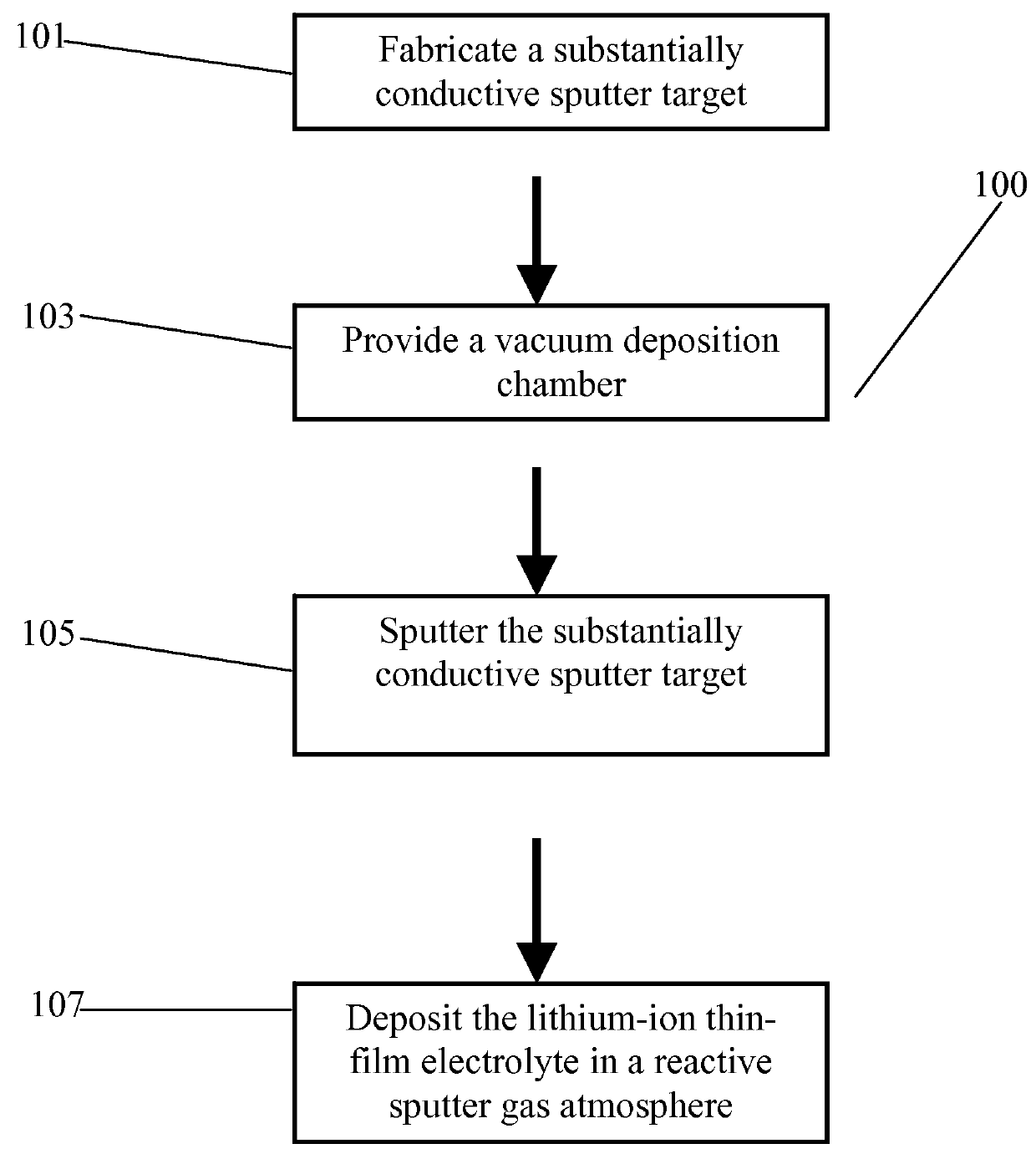
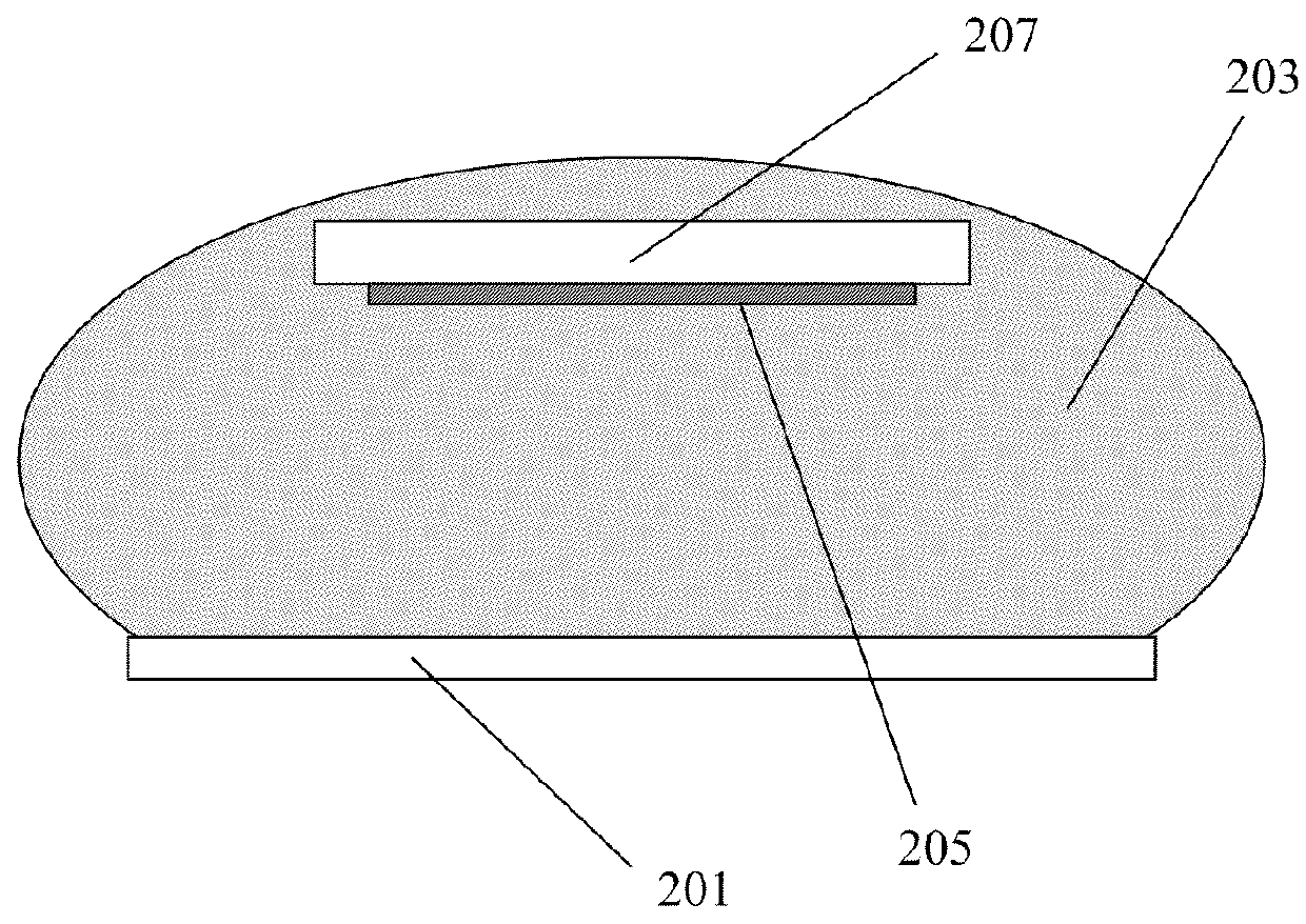
[0041]Example 1 (FIG. 2) provides an exemplary embodiment of process 100 in which a LIPON electrolyte film of composition Li2.9PO3.3N0.46 205 may be deposited onto a substrate 207 by DC, pulsed DC, AC, or RF reactive sputtering from semi-conducting target of the composition Li3P 201 when immersed in a sputter plasma plume 203 including the sputtered material and a reactive gas mixture of oxygen and nitrogen, with or without addition of inert gas such as argon. The O2 / N2 ratio is to be adapted to less than 1 / 100 due to the much higher affinity of the depositing Li and P species to bond with oxygen compared to nitrogen. For a given oxygen / nitrogen ratio (for example, 1 / 1000) inside the vacuum deposition reactor both kinetic and thermodynamic factors determine the final stoichiometric parameters x, y, and z in the growing LixPOyNz film. Among the kinetic parameters are the target sputter power (for example, 2000 W for 10 inch in diameter Li3P target), the pulsed duty cycle (for example...

example 2 (fig.3)

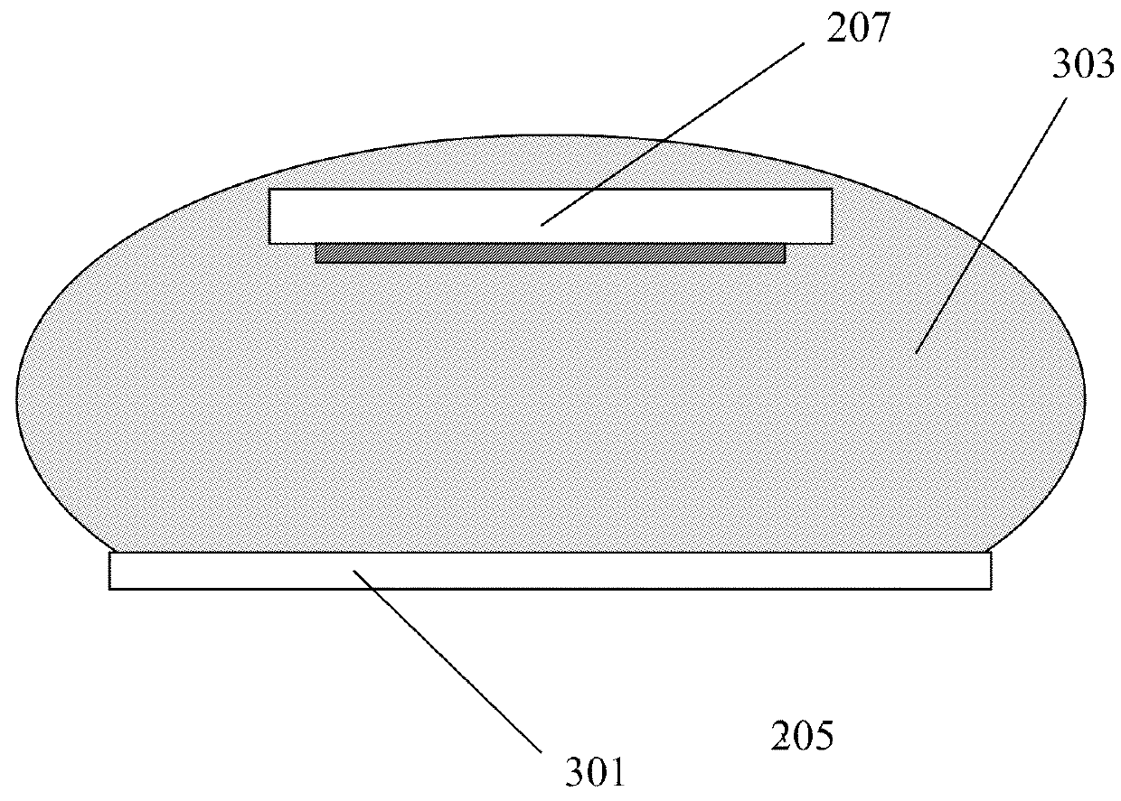
[0042]Example 2 (FIG. 3) provides an exemplary embodiment of process 100 in which a LIPON electrolyte film of Li2.9PO3.3N0.46 205 may be deposited by DC, pulsed DC, AC, or RF reactive sputtering from a composite target 301 composed of lithium rich LixP (x>>3) 305 and Li2O, 307 either composited on a microscopic level or on a centimeter scale by alternatingly placing LixP tiles and Li2O tiles substantially close to each other so that when sputtering such target in a reactive, at least nitrogen containing sputter plasma plume 303, with or without addition of inert gas such as argon, the concentration ratio of Li / P yields about 2.9, the O / P ratio yields about 3.3, while the N / P ratio amounts to about 0.46. The microscopic composition of LixP (x>>3) 305 and Li2O 307 may be preferred over the centimeter scale composite, because it provides a semi-conducting surface of the sputter target 301 that is useful for operating the target under DC or pulse sputter conditions.

[0043]Example 3 (FIG....

example 4

[0044 provides an exemplary embodiment of process 100 in which the sputter target comprises P2O5 instead of LixP (x>>3) as provided by Example 3 (FIG. 4) and the so-fabricated sputter target is DC, pulsed DC, AC, or RF sputtered in an atmosphere containing at least nitrogen.

[0045]Example 5 provides an exemplary embodiment of process 100 in which the sputter target comprises PN instead of P2O5 as provided by Example 4 and the so-fabricated sputter target is DC, pulsed DC, AC, or RF sputtered in an atmosphere containing at least nitrogen and oxygen.

[0046]Example 6 provides an exemplary embodiment of process 100 in which the sputter target is fabricated from a microscopic composite of metallic lithium and PN and the so-fabricated sputter target is DC, pulsed DC, AC, or RF sputtered in an atmosphere containing at least nitrogen and oxygen.


PUM

PropertyMeasurementUnit
electronic conductivityaaaaaaaaaa
frequencyaaaaaaaaaa
frequencyaaaaaaaaaa

Abstract

Alternative sputter target compositions or configurations for thin-film electrolytes are proposed whereby the sputter target materials system possesses sufficient electrical conductivity to allow the use of (pulsed) DC target power for sputter deposition. The electrolyte film materials adopt their required electrically insulating and lithium-ion conductive properties after reactive sputter deposition from the electrically conducting sputter target materials system.

Description

RELATED APPLICATIONS[0001]This application is related to and claims the benefit under 35 U.S.C. §119 of U.S. provisional application Ser. No. 61 / 016,038, entitled “METHOD FOR SPUTTER TARGETS FOR ELECTROLYTE FILMS,” filed Dec. 21, 2007, which is incorporated herein by reference in its entirety.FIELD OF THE INVENTION[0002]The present invention is related to the fabrication of lithium-ion thin-film electrolytes for use in thin-film electrochemical energy storage and conversion devices.BACKGROUND OF THE INVENTION[0003]Presently, lithium-ion electrolyte layers are deposited from ceramic, insulating sputter targets using radio-frequency (RF) excitation (1 MHz-1 GHz) on the sputter target together with a RF tuner and a RF matching network. The main reason for this approach lies in the fact that the ceramic target composition or stoichiometry can be fabricated identical, or at least most similar, to the stochiometry of the lithium-ion electrolyte layer to be deposited. However, both the use...

Claims


Application Information

Patent Timeline
Patent Type & Authority Patents(United States)
IPC IPC(8): C23C14/38C23C14/22C23C14/00C23C14/06C23C14/34C23C14/35H01M2/14H01M6/18H01M6/40H01M10/0525H01M10/0562H01M10/058
CPCC23C14/06C23C14/0036C23C14/22C23C14/3407C23C14/3414C23C14/352H01M2/145H01M6/188H01M6/40H01M10/0525H01M10/0562H01M10/058Y02E60/122Y02P70/54Y02P70/50Y02E60/10
Inventor NEUDECKER, BERND J.WHITACRE, JAY F.
Owner SAPURAST RES
Learn More