Output buffer circuit, array substrate and display device

a display device and array substrate technology, applied in the field of output buffer circuits, can solve the problems of increasing the requirement for the power consumption of increasing the requirement for the power consumption of the driving control chip and the image quality of the liquid crystal screen, so as to achieve good stability and suppress the fluctuation of output voltage

Active Publication Date: 2016-05-17
BOE TECH GRP CO LTD +1
View PDF6 Cites 0 Cited by
  • Summary
  • Abstract
  • Description
  • Claims
  • Application Information

AI Technical Summary

Benefits of technology

[0008]The embodiments of present invention provide an output buffer circuit, an array substrate and a display device, to suppress fluctuation of the output voltage of the output buffer circuit, such that the output voltage has good stability.

Problems solved by technology

However, in the display field of the prior art, the power consumption of the entire voltage driving circuit of the displayer is becoming larger and larger with higher requirement for the resolution and the pixel quality of the displayer, thus the requirement for the power consumption of the driving control chip and the image quality of the liquid crystal screen is becoming higher and higher.
The requirement for the power consumption of the liquid crystal screen is higher and higher with the size of the liquid crystal screen becoming larger and larger.
Since there is no feedback circuit provided in the output buffer circuit shown in the above FIG. 1, suppression of output fluctuations of the output buffer circuit may not be realized, thus the output voltage will have high fluctuation and low stability.
In order to solve the problem of the instable output, a conventional output buffer circuit generally needs a special voltage stabilizing circuit in addition to the above two-stage operational amplifying circuit, thus the area of the chip is increased, a bias current of the output stage is needed to be increased at the meantime to increase the sink current to the load, and the power consumption is increased.

Method used


Image

  • Output buffer circuit, array substrate and display device
  • Output buffer circuit, array substrate and display device
  • Output buffer circuit, array substrate and display device

Examples


Embodiment Construction

[0019]The technical solutions in the embodiments of the present invention will be described clearly and completely hereinafter with reference to the attached drawings in the embodiments of the present invention. Apparently, the described embodiments are only part of the exemplary embodiments of the present invention and are not tended to covering all of the embodiments.

[0020]In addition, in the following detailed description, for the purposes of convenient explanation, numerous specific details are set forth in order to provide a thorough understanding of the disclosed embodiments. It will be apparent, however, that one or more embodiments may be practiced without these specific details. In other instances, well-known structures and devices are schematically shown in order to simplify the drawings.

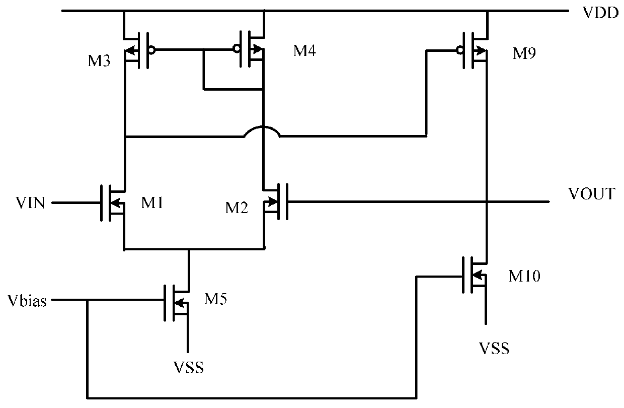
[0021]Currently, a normal output voltage of an output buffer circuit for providing the driving voltage VOFF of TFT-LCD gate driver is about −8V, and a voltage stabilizing capacitor needs t...


PUM


Abstract

The embodiments of the present invention provide a output buffer circuit, comprising: a first stage operational amplifying circuit configured as a differential input circuit; a second stage operational amplifying circuit configured as a common source amplifying circuit having an active load; and a feedback circuit provided between the first stage operational amplifying circuit and the second stage operational amplifying circuit and configured to have driving capability of providing source current and sink current alternately. By forming a unit gain amplifier comprising the first stage operational amplifying circuit, the second stage operational amplifying circuit and the feedback circuit connected therebetween, the output buffer circuit has the driving capability of providing source current and sink current alternately. No special voltage stabilizing circuit is needed, thus the circuit structure is simple and the chip area is decreased; since the power consumption can be reduced without a special voltage stabilizing circuit, the fluctuation of the output voltage is suppressed at the same time, the stability of the circuit is ensured in operation and offset is suppressed optimally, the output signal is more accurate and the quality of image displayed is improved.

Description

CROSS-REFERENCE TO RELATED APPLICATION[0001]This application claims the benefit of Chinese Patent Application No. 201410046370.9 filed on Feb. 10, 2014 in the State Intellectual Property Office of China, the whole disclosure of which is incorporated herein by reference.BACKGROUND OF THE INVENTION[0002]1. Field of the Invention[0003]Embodiments of present invention relate to the field of liquid crystal display, and in particular, to an output buffer circuit, an array substrate and a display device.[0004]2. Description of the Related Art[0005]Liquid crystal displayers are widely used because of its portable, ultrathin, multicolor and high definition characteristics. However, in the display field of the prior art, the power consumption of the entire voltage driving circuit of the displayer is becoming larger and larger with higher requirement for the resolution and the pixel quality of the displayer, thus the requirement for the power consumption of the driving control chip and the ima...

Claims


Application Information

Patent Timeline
Patent Type & Authority Patents(United States)
IPC IPC(8): H03F1/02H03F3/45G09G3/36
CPCH03F1/0261G09G3/3677H03F3/45183G09G2310/0291H03F2203/45674
Inventor LIU, BAOYUZHANG, LIANGXU, YIZHENSUN, ZHIHUA
Owner BOE TECH GRP CO LTD
Why Eureka
Try Eureka