Apparatus and method for sense amplifier offset cancellation

an amplifier and offset cancellation technology, applied in the field of electronic circuitry, can solve problems such as incongruity in practice, and achieve the effect of sacrificing bandwidth

Active Publication Date: 2016-07-05
TAHOE RES LTD
View PDF4 Cites 7 Cited by
  • Summary
  • Abstract
  • Description
  • Claims
  • Application Information

AI Technical Summary

Benefits of technology

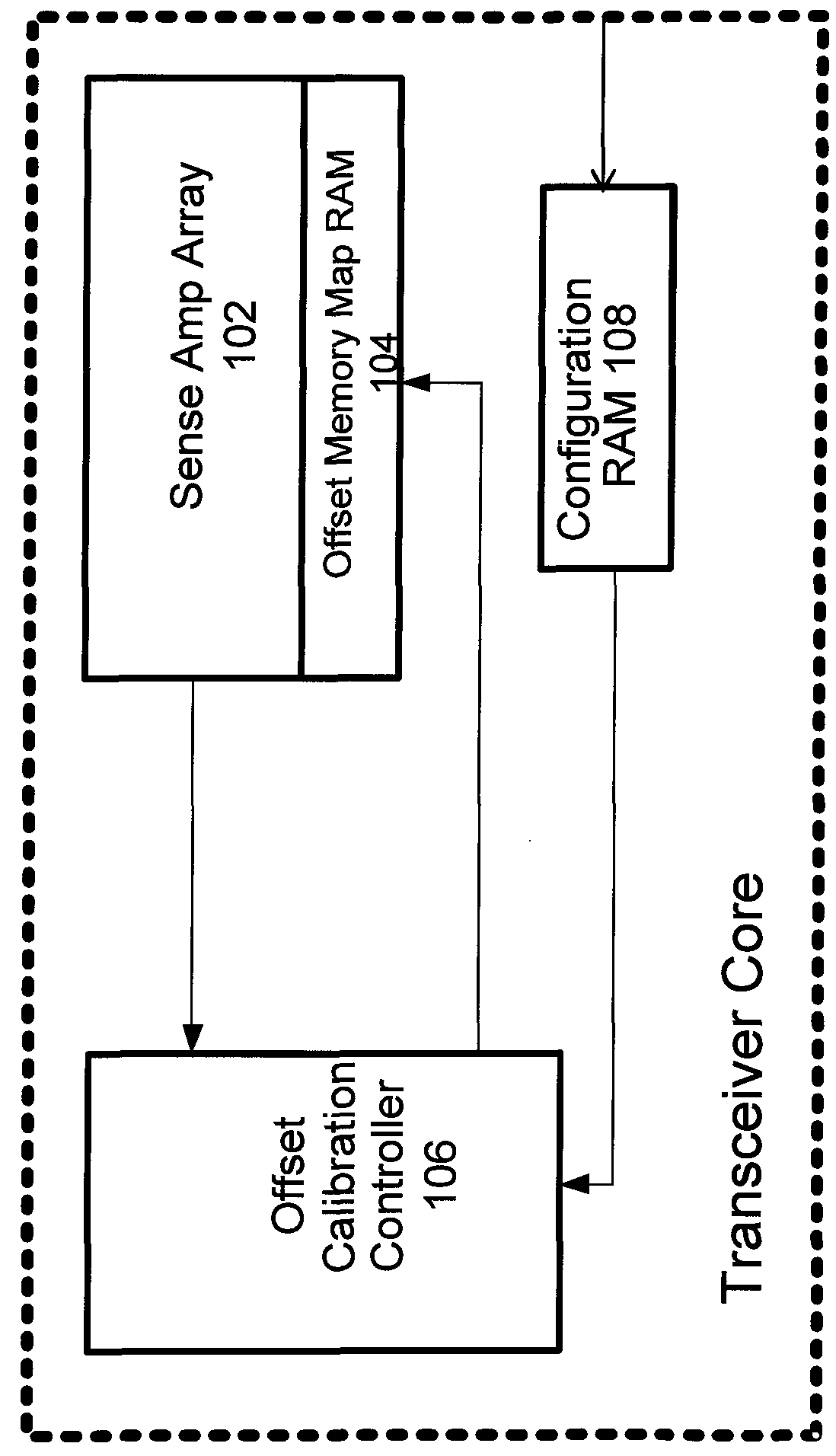
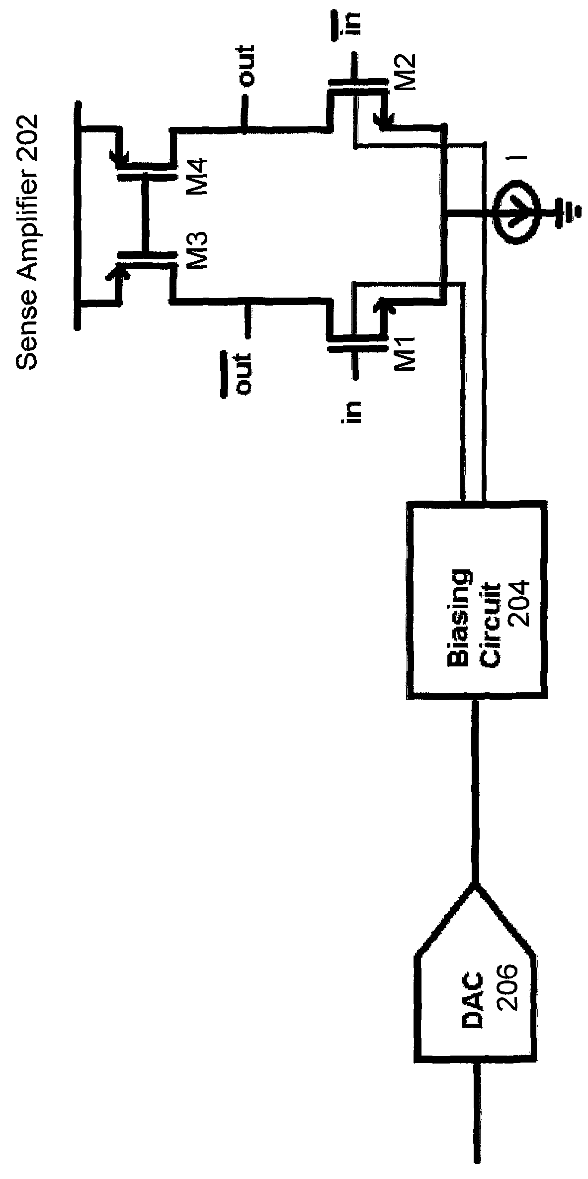
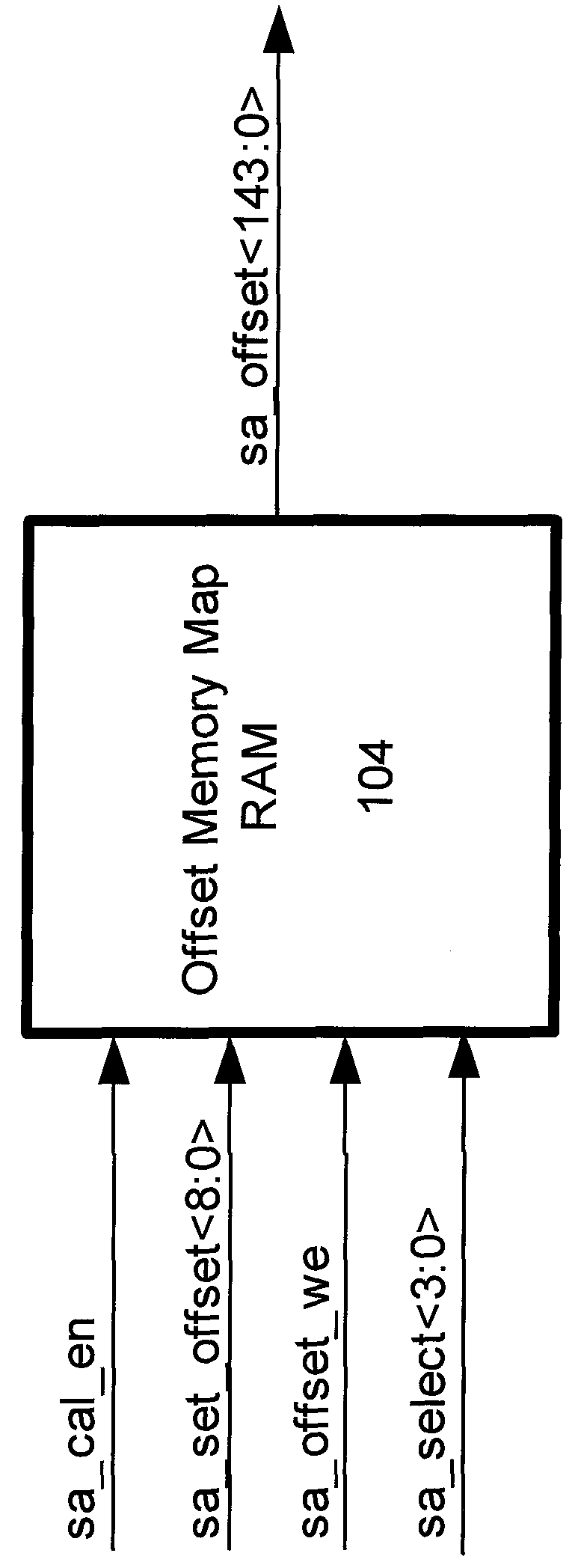
[0005]Disclosed is a circuit architecture for cancellation of threshold voltage offsets for an array of sense amplifiers. An offset calibration controller, which may be embedded as a hard-wired circuit in the transceiver core circuits, writes the offset adjustment values to a memory-mapped interface circuit. The memory-mapped interface circuit outputs the offset adjustment values to offset adjustment circuits for the sense amplifiers. The offset adjustment circuits may utilize a body bias technique. Advantageously, the disclosed circuit architecture provides for the minimization of residual offset without sacrificing bandwidth.

Problems solved by technology

While the two transistors of the input differential pair are generally designed to be the same, they are often not identical in practice due to process variation during manufacture.

Method used


Image

  • Apparatus and method for sense amplifier offset cancellation
  • Apparatus and method for sense amplifier offset cancellation
  • Apparatus and method for sense amplifier offset cancellation

Examples


example fpga

[0045]FIG. 5 is a simplified partial block diagram of a field programmable gate array (FPGA) 1 that can include aspects of the present invention. In one embodiment, the integrated circuit on which transceiver core 100 is implemented may be such an FPGA. It should be understood that, in accordance with other embodiments, the present invention may be implemented and used in numerous types of integrated circuits such as field programmable gate arrays (FPGAs), programmable logic devices (PLDs), complex programmable logic devices (CPLDs), programmable logic arrays (PLAs), digital signal processors (DSPs) and application specific integrated circuits (ASICs).

[0046]FPGA 1 includes within its “core” a two-dimensional array of programmable logic array blocks (or LABs) 2 that are interconnected by a network of column and row interconnect conductors of varying length and speed. LABs 2 include multiple (e.g., ten) logic elements (or LEs).

[0047]An LE is a programmable logic block that provides fo...

example digital

System

[0051]FIG. 6 shows a block diagram of an exemplary digital system 50 that can embody techniques of the present invention. System 50 may be a programmed digital computer system, digital signal processing system, specialized digital switching network, or other processing system. Moreover, such systems can be designed for a wide variety of applications such as telecommunications systems, automotive systems, control systems, consumer electronics, personal computers, Internet communications and networking, and others. Further, system 50 may be provided on a single board, on multiple boards, or within multiple enclosures.

[0052]System 50 includes a processing unit 52, a memory unit 54, and an input / output (I / O) unit 56 interconnected together by one or more buses. According to this exemplary embodiment, FPGA 58 is embedded in processing unit 52. FPGA 58 can serve many different purposes within the system 50. FPGA 58 can, for example, be a logical building block of processing unit 52,...


PUM


Abstract

Disclosed is a circuit architecture for cancellation of threshold voltage offsets for an array of sense amplifiers. An offset calibration controller, which may be embedded as a hard-wired circuit in the transceiver core circuits, writes the offset adjustment values to a memory-mapped interface circuit. The memory-mapped interface circuit outputs the offset adjustment values to offset adjustment circuits for the sense amplifiers. The offset adjustment circuits may utilize a body bias technique. Advantageously, the disclosed circuit architecture provides for the minimization of residual offset without sacrificing bandwidth. Other embodiments, features and advantages are also disclosed.

Description

BACKGROUND[0001]1. Technical Field[0002]The present invention relates generally to electronic circuitry. More particularly, the present invention relates to apparatus and methods for sense amplifier offset cancellation.[0003]2. Description of the Background Art[0004]A sense amplifier may be used to amplify a differential signal across two inputs. While the two transistors of the input differential pair are generally designed to be the same, they are often not identical in practice due to process variation during manufacture. In particular, the process variation may cause the two transistors of the input differential pair to have different threshold voltages. In that case, the sense amplifier may be said to have an offset at the two inputs caused by the mismatch between the two transistors.SUMMARY[0005]Disclosed is a circuit architecture for cancellation of threshold voltage offsets for an array of sense amplifiers. An offset calibration controller, which may be embedded as a hard-wi...

Claims


Application Information

Patent Timeline
Patent Type & Authority Patents(United States)
IPC IPC(8): G11C7/06G11C7/10
CPCG11C7/06G11C7/1051G11C7/08G11C2207/2254
Inventor CHAN, ALLEN K.GIRIDHARAN, VISHALBAHADUR, SYED REZA
Owner TAHOE RES LTD
Why Eureka
Try Eureka