
Two-dimensional APDs and SPADs and related methods

a two-dimensional apd and spad technology, applied in the field of two-dimensional apds and spads, can solve the problems of reducing the performance of the remaining layers, placing limitations on the design of apds or spads,

Active Publication Date: 2016-07-12
NAT TECH & ENG SOLUTIONS OF SANDIA LLC
View PDF6 Cites 40 Cited by
  • Summary
  • Abstract
  • Description
  • Claims
  • Application Information

AI Technical Summary

Benefits of technology

The patent text describes a device called an avalanche photodiode (APD) that can convert optical signals into electrical signals. It can amplify the signal so much that it is easier to measure. This makes it very sensitive and can detect extremely small amounts of light. The technical effect of this invention is that it provides a better way to measure optical signals and has applications in various fields such as optical communication and detection.

Problems solved by technology

However, the use of a stack of layers places limitations on the design of an APD or SPAD.
For example, certain design modifications that may improve the operation of one layer may degrade the performance of the remaining layers.

Method used


Image

  • Two-dimensional APDs and SPADs and related methods
  • Two-dimensional APDs and SPADs and related methods
  • Two-dimensional APDs and SPADs and related methods

Examples


Embodiment Construction

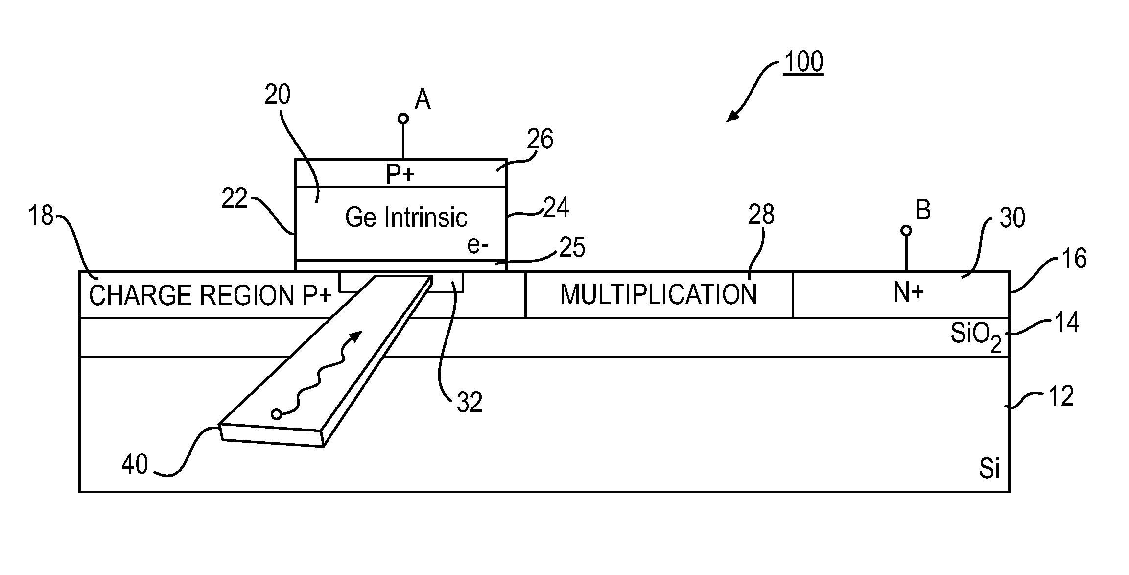
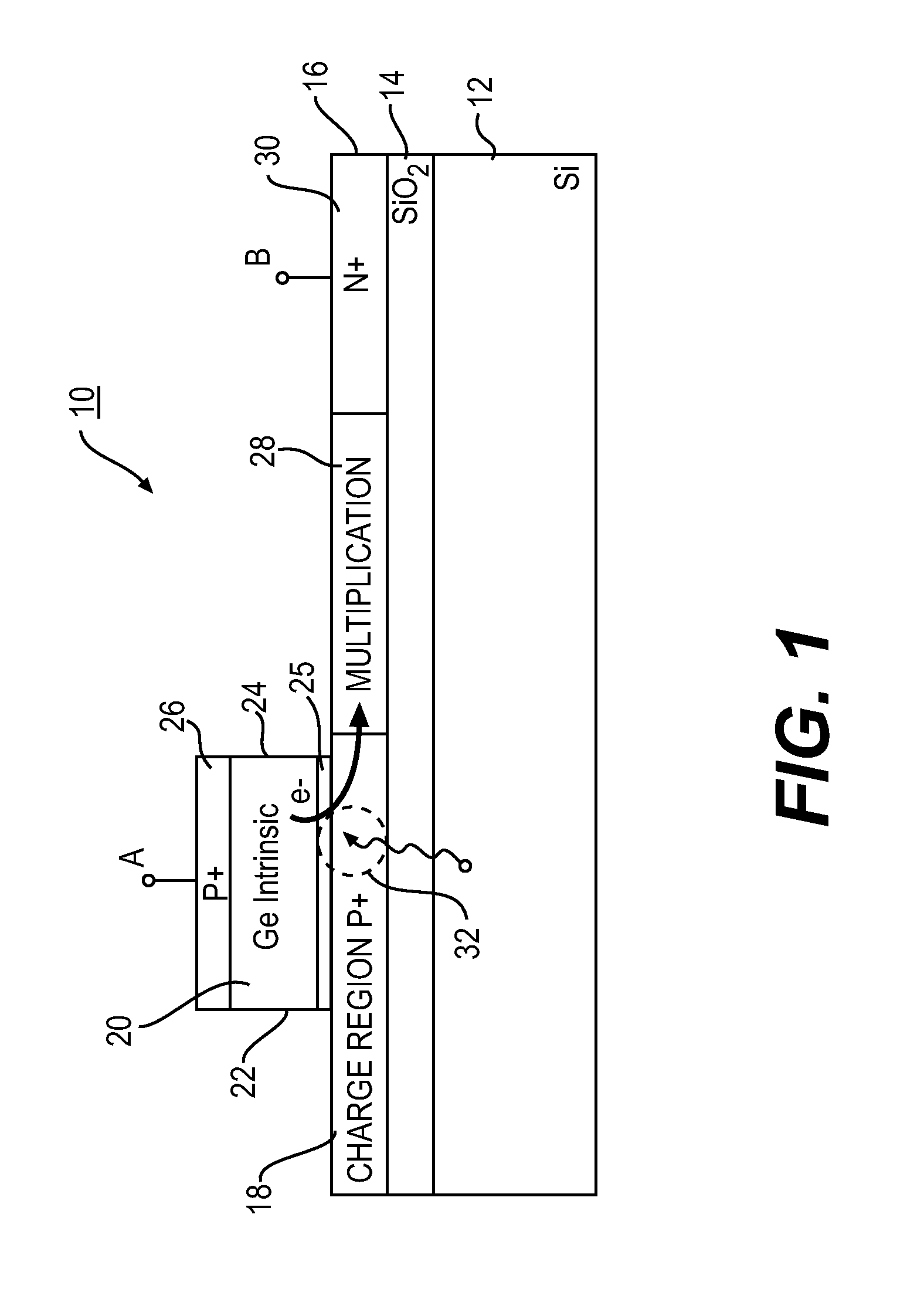
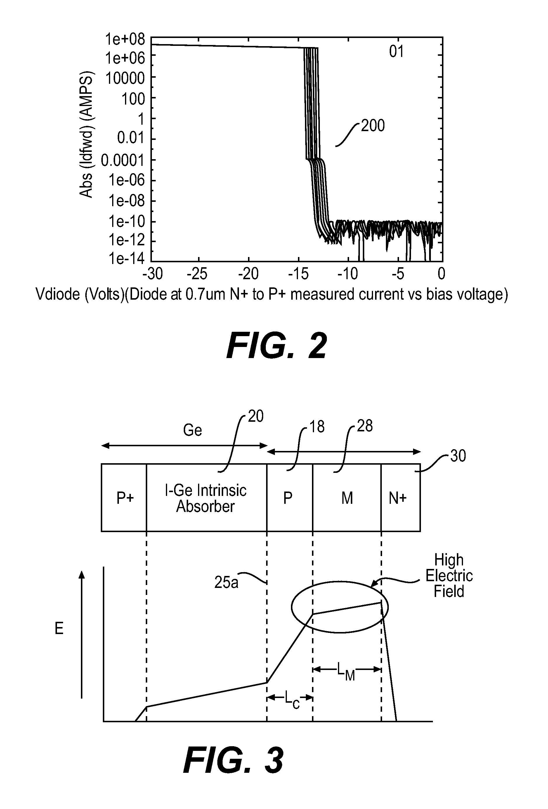
[0028]Exemplary embodiments of two-dimensional optical devices, such as APDs and SPADs, and related methods are described herein in detail and shown by way of example in the drawings. Throughout the following description and drawings, like reference numbers / characters refer to like elements. It should be understood that, although specific exemplary embodiments are discussed herein there is no intent to limit the scope of present invention to such embodiments. To the contrary, it should be understood that the exemplary embodiments discussed herein are for illustrative purposes, and that modified and alternative embodiments may be implemented without departing from the scope of the present invention.

[0029]It should be further noted that some exemplary embodiments may be described and claimed as a process or method (hereafter “method”). Though a method may be described and claimed as set of sequential steps, it should be understood that the steps may be performed in parallel, concurren...


PUM


Abstract

Avalanche photodiodes (APDs) and single photon avalanche detectors (SPADs) are provided with a lateral multiplication region that provides improved amplification through increased impact ionization.

Description

GOVERNMENT LICENSE RIGHTS[0001]This invention was developed under Contract DE-AC04-94AL85000 between Sandia Corporation and the U.S. Department of Energy. The U.S. Government has certain rights in this invention.INTRODUCTION[0002]Avalanche photodiodes (APDs) may be used to convert optical signals into amplified, electrical signals. Due to their ability to greatly amplify a received signal, APDs may be used as very sensitive detectors that permit optical signals of extremely low power to be received, and then converted into amplified (higher power) electrical signals that are more easily measured.[0003]When operated in a so-called “Geiger mode”, APDs may be used to receive and measure a single photon. These devices may also be referred to as “single photon avalanche detectors” (SPADs).[0004]Typically, APDs as well as SPADs may be formed as a layered “stack” of various semiconductor materials. APDs and SPADS that use this stacked configuration may be referred to as “one dimensional” A...

Claims


Application Information

Patent Timeline
Patent Type & Authority Patents(United States)
IPC IPC(8): G01J1/42G02B6/24G02B6/10H01L31/107H01L31/02G02B6/02
CPCH01L31/1075G02B6/02G02B6/10H01L31/107G02B6/24H01L31/02027G02B6/12004G02B2006/12061G02B2006/12123H01L31/165
Inventor DAVIDS, PAULTROTTER, DOUGLAS CHANDLERDEROSE, CHRISTOPHER
Owner NAT TECH & ENG SOLUTIONS OF SANDIA LLC
Learn More