Array substrate, method for fabricating the same, and OLED display device

a technology of array substrate and substrate, applied in the direction of diodes, organic semiconductor devices, semiconductor devices, etc., can solve the problems of high cost and complicated fabrication process, and achieve the effects of low cost, high cost and simple fabrication process

Active Publication Date: 2016-07-26
BOE TECH GRP CO LTD
View PDF12 Cites 9 Cited by
  • Summary
  • Abstract
  • Description
  • Claims
  • Application Information

AI Technical Summary

Benefits of technology

[0009]Technical problems to be solved by the present invention include: providing an array substrate with simple fabrication process, and low cost, in view of the problem that array substrates with microcavity structures have complicated fabrication process and high cost in the prior art.

Problems solved by technology

However, the inventors find that at least the following problem exists in the prior art: the respective anodes of the array substrate are disposed in the same layer and may be originally formed in a single patterning process at the same time.
However, in a WOLED display device having microcavity structures, the anodes of respective pixel units are of different thicknesses, and therefore they are separately formed in a plurality of patterning processes, or a dual-tone mask needs to be used in the patterning process, while these methods lead to complicated fabrication process and high cost.

Method used


Image

  • Array substrate, method for fabricating the same, and OLED display device
  • Array substrate, method for fabricating the same, and OLED display device
  • Array substrate, method for fabricating the same, and OLED display device

Examples


embodiment 1

[0060

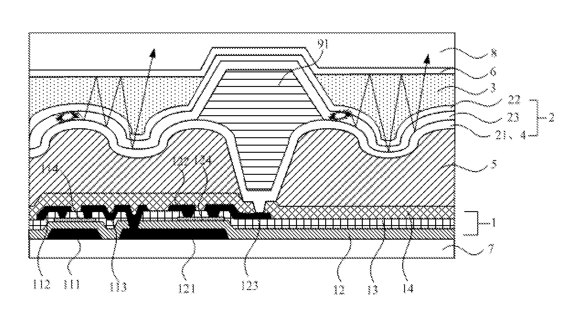
[0061]As shown in FIG. 3, the present embodiment provides an array substrate, which comprises a plurality of pixel units disposed on a substrate 7; and each pixel unit comprises:

[0062]a TFT drive layer 1;

[0063]an OLED 2 further away from the substrate 7 than the TFT drive layer 1 and driven by it, the OLED 2 sequentially comprising a first electrode 21, a light emitting layer 23, and a transparent second electrode 22 in a direction away from the substrate 7, wherein the first electrode 21 is a reflection layer 4, or the first electrode 21 is transparent and has a reflection layer 4 disposed thereunder;

[0064]a transflective layer 6 further away from the substrate 7 than the OLED 2 and forming a microcavity structure with the reflection layer 4; and

[0065]a color filter film 3 disposed between the OLED 2 and the transflective layer 6 and located in the microcavity structure.

[0066]In the array substrate of the present embodiment, the color filter film 3 is disposed in the microcavi...

embodiment 2

[0067

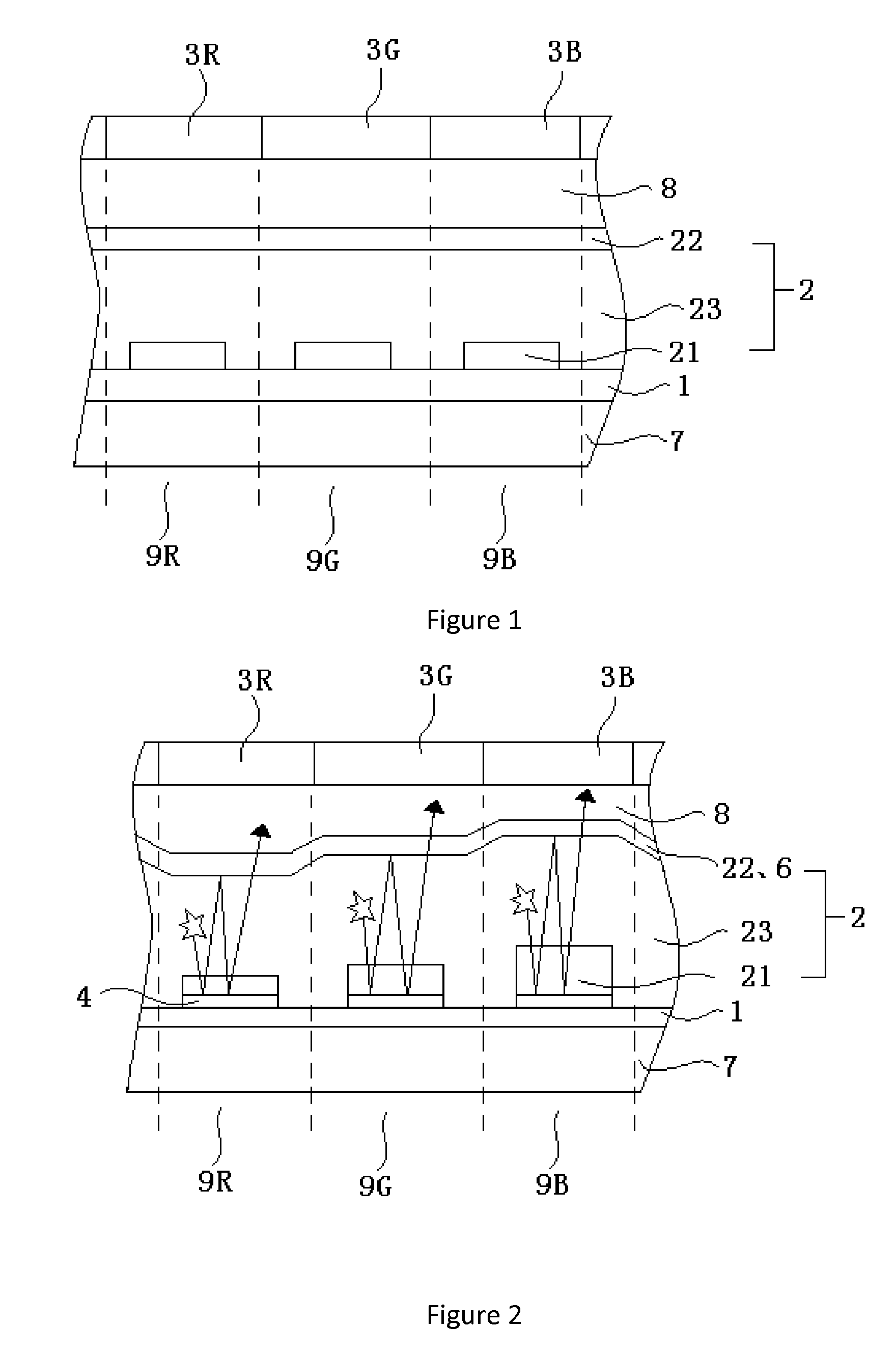
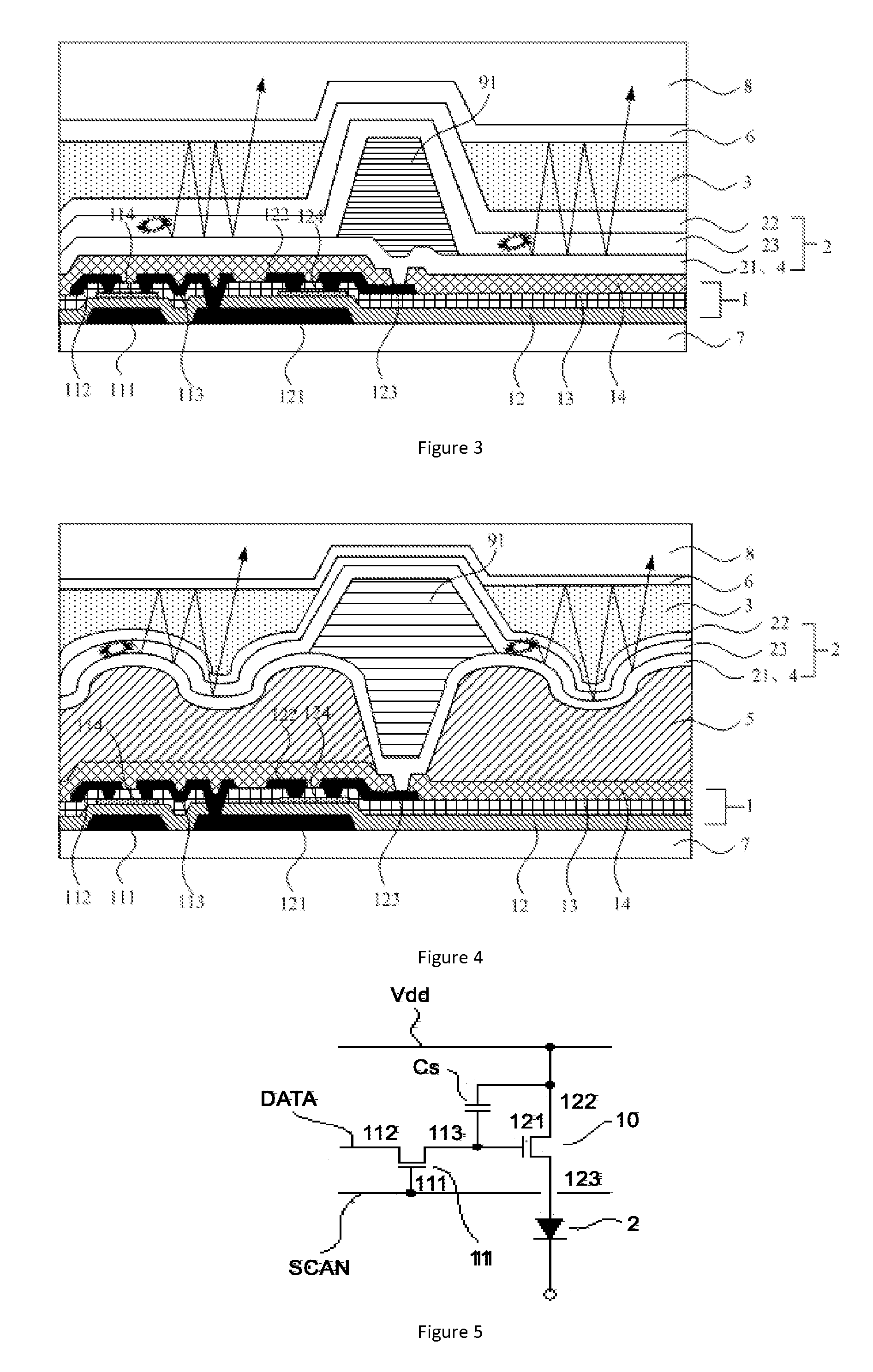
[0068]As illustrated in FIGS. 4 and 5, the present embodiment provides an array substrate, which comprises a plurality of pixel units on a substrate 7, wherein a plurality of adjacent pixel units having color filter films of different colors form one ‘visible pixel’ on a display. Herein a color filter film may have various color modes. Preferably, the color filter film comprises a red filter film, a green filter film, a blue filter film (the RGB mode). Alternatively, the color filter film comprises a red filter film, a green filter film, a blue filter film and a white filter film (the RGBW mode). Alternatively, the color filter film comprises a red filter film, a green filter film, a blue filter film and a yellow filter substrate (the RGBY mode).

[0069]As illustrated in FIG. 4, the array substrate sequentially comprises a TFT drive layer 1, a resin layer 5. an OLED 2, a color filter film 3, and an encapsulation layer 8 in a direction further away from the substrate 7.

[0070]The T...

embodiment 3

[0095

[0096]The present embodiment provides a method for fabricating an array substrate, which comprises the following steps:

[0097]forming a pattern comprising a TFT drive layer on a substrate;

[0098]forming a pattern comprising an OLED on the subject subjected to the previous step, wherein a second electrode of the OLED away from the substrate is transparent, and a first electrode of the OLED close to the substrate is a reflection layer, or a first electrode of the OLED close to the substrate is transparent and a reflection layer is disposed thereunder;

[0099]forming a pattern comprising a color filter film on the substrate subjected to the previous step; and

[0100]forming a pattern comprising a transflective layer on the substrate subjected to the previous step.

[0101]In an array substrate fabricated according to the method of the present invention, the color filter film is disposed in the microcavity structure, and therefore thickness of the microcavity structure may be adjusted by re...


PUM


Abstract

This invention provides an array substrate, a method for fabricating the same, and an OLED display device, which can solve the technical problem that the existing OLED display device has low luminous efficiency. Each pixel unit of the array substrate comprises: a TFT drive layer; an OLED further away from the substrate than the TFT drive layer and driven by it, the OLED sequentially comprises a first electrode, a light emitting layer, and a transparent second electrode, wherein the first electrode is a reflection layer, or the first electrode is transparent and has a reflection layer disposed thereunder; a transflective layer further away from the substrate than the OLED and forming a microcavity structure with the reflection layer; and a color filter film disposed between the OLED and the transflective layer and located in the microcavity structure. The present invention is particularly suitable for a WOLED display device.

Description

FIELD OF THE INVENTION[0001]The present invention relates to the field of OLED display technology, more particularly, to an array substrate, a method for fabricating the same and an OLED display device.BACKGROUND OF THE INVENTION[0002]An Organic Light Emitting Diode (OLED) is an organic thin film electroluminescent (EL) device, which has advantages of simple fabrication process, low cost, high luminous efficiency and easy formation of flexible structure. Therefore, display technology employing an OLED has become important display technology.[0003]An OLED display device comprises a plurality of pixel units, each of which has an OLED disposed therein. The luminous intensity of each OLED is controlled by controlling current flowing through the OLED, thereby realizing image display. Herein, each visible pixel on a display is made of a plurality of adjacent pixel units emitting light of different colors, and light emitted from the respective pixel units is mixed to form light emitted fro...

Claims


Application Information

Patent Timeline
Patent Type & Authority Patents(United States)
IPC IPC(8): H01L29/08H01L27/32H01L51/52H01L51/56
CPCH01L27/3248H01L27/322H01L27/3258H01L51/5209H01L51/5265H01L51/5271H01L51/56H01L27/3206H01L27/3272H01L2251/5315H10K59/30H10K59/38H10K59/123H10K59/124H10K59/126H10K50/813H10K50/852H10K50/856H10K2102/3026H10K71/00
Inventor SONG, YOUNGSUKYOO, SEONGYEOLCHOI, SEUNGJINKIM, HEECHEOL
Owner BOE TECH GRP CO LTD
Why Eureka
Try Eureka