
Monolithic composite resonator devices with reduced sensitivity to acceleration and vibration

a composite resonator, acceleration acceleration technology, applied in the direction of oscillator generators, instruments, impedence convertors, etc., can solve the problems of insufficient high q, difficult to achieve high-quality (i.e., high-q) inductors using conventional wafer-scale fabrication techniques, and relatively low resistivity

Active Publication Date: 2016-08-30
INTEGRATED DEVICE TECH INC
View PDF20 Cites 6 Cited by
  • Summary
  • Abstract
  • Description
  • Claims
  • Application Information

AI Technical Summary

Benefits of technology

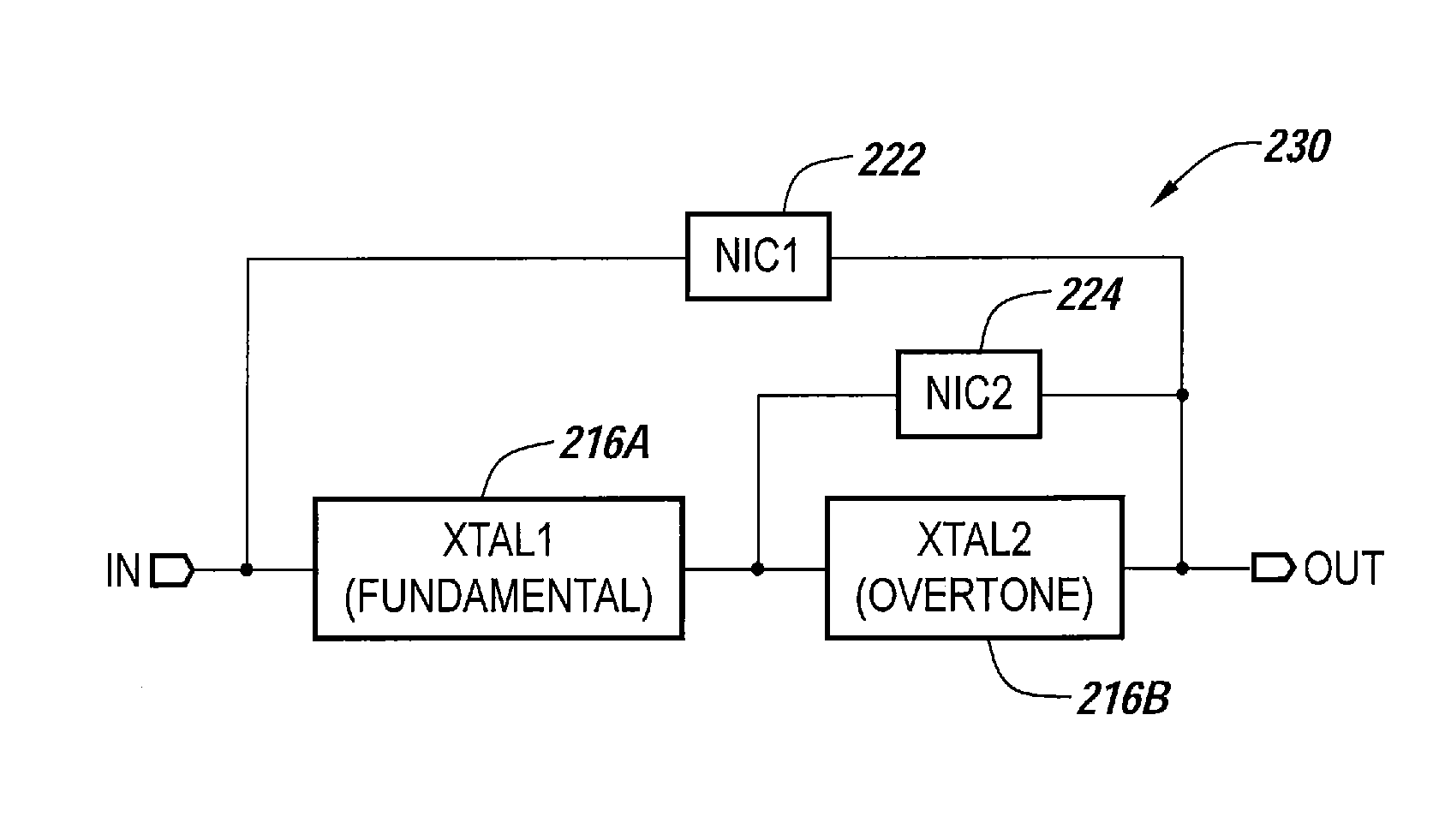
The invention relates to integrated circuit devices that include a plurality of serially-connected resonators and a programmable negative impedance converter (NIC). The NIC is designed to mimic a negative capacitive reactance and is responsive to a reference voltage that changes in response to changes in temperature. The NIC can be connected to the output of one of the resonators or to both resonators simultaneously. The NIC can also be programmed to weight the acceleration vector of one of the resonators relative to the other. The invention also includes a monolithic multi-resonator device that includes two quartz resonators connected in series and an integrated circuit substrate with a programmable NIC. The technical effects of the invention include improved performance and stability of the integrated circuit devices, as well as reduced susceptibility to acceleration forces.

Problems solved by technology

However, achieving high-quality (i.e., high-Q) inductors can often be difficult using conventional wafer-scale fabrication techniques.
Moreover, because inductors create surrounding fields, forming inductors adjacent lossy materials will significantly reduce their Q. Accordingly, high value inductors, such as spiral inductors, may provided insufficiently high Q when formed on an integrated circuit (IC) substrate having relatively low resistivity.

Method used


Image

  • Monolithic composite resonator devices with reduced sensitivity to acceleration and vibration
  • Monolithic composite resonator devices with reduced sensitivity to acceleration and vibration
  • Monolithic composite resonator devices with reduced sensitivity to acceleration and vibration

Examples


Embodiment Construction

[0056]The present invention now will be described more fully with reference to the accompanying drawings, in which preferred embodiments of the invention are shown. This invention may, however, be embodied in many different forms and should not be construed as being limited to the embodiments set forth herein; rather, these embodiments are provided so that this disclosure will be thorough and complete, and will fully convey the scope of the invention to those skilled in the art. Like reference numerals refer to like elements throughout.

[0057]It will be understood that, although the terms first, second, third, etc. may be used herein to describe various elements, components, regions, layers and / or sections, these elements, components, regions, layers and / or sections should not be limited by these terms. These terms are only used to distinguish one element, component, region, layer or section from another region, layer or section. Thus, a first element, component, region, layer or sec...


PUM


Abstract

An integrated circuit device includes a pair of serially-connected crystal resonators arranged as a first crystal resonator, which is configured to preferentially support a fundamental resonance mode in response to an input signal, and a second crystal resonator, which is configured to preferentially support a third or higher overtone resonance mode in response to a signal generated at an output terminal of the first crystal resonator. A negative impedance converter (NIC) is also provided, which has an input terminal electrically connected to an input terminal of the first crystal resonator and an output terminal electrically connected to one of the output terminal of the first crystal resonator and the output terminal of the second crystal resonator. The NIC may be a CMOS-based NIC that is devoid of inductive reactance from a passive inductor.

Description

CROSS-REFERENCE TO RELATED APPLICATION[0001]This application is related to U.S. application Ser. No. 14 / 871,411, filed Sep. 30, 2015, entitled “Packaged Oscillators With Built-In Self-Test Circuits that Support Resonator Testing with Reduced Pin Count,” and U.S. application Ser. No. 14 / 586,508, filed Dec. 30, 2014, entitled “Integrated Circuit Device Substrates Having Packaged Crystal Resonators Thereon,” now U.S. Pat. No. 9,306,537, the disclosures of which are hereby incorporated herein by reference.FIELD OF THE INVENTION[0002]The present invention relates to integrated circuit devices and methods of forming same and, more particularly, to resonator devices and oscillator circuits and methods of forming same on integrated circuit substrates.BACKGROUND OF THE INVENTION[0003]Current state-of-the art microelectromechanical (MEMs) resonators have recently challenged the quartz-dominated timing industry, notwithstanding the perceived temperature instabilities of such MEMs devices, whic...

Claims


Application Information

Patent Timeline
IPC IPC(8): H03B5/04H03H9/13H03H9/205H03B5/32H03H9/10
CPCH03B5/04H03B5/32H03H9/13H03H9/205H03H9/10H03H9/02133H03H9/02834H03H9/02897H03H9/0547H03H9/1021H03H11/44H03B5/36G01R31/282G01R31/2836G01R31/2853G01R31/2884
Inventor NORTHCUTT, JAMES BRYANTREFETHEN, EUGENE STANLEYSUTTER, HARRY LEROYTIBBITTS, STEPHEN AMARRICE, CHARLES MICHAELCLARK, BRUCE EDWARD
Owner INTEGRATED DEVICE TECH INC
Learn More