Method and compound system for inspecting and reviewing defects

a technology of inspection and inspection apparatus, applied in the direction of electrical equipment, electric discharge tubes, basic electric elements, etc., can solve the problems of inability to observe the optical inspection tool, the dimension of the defect is smaller than the optical wavelength, and the conventional optical inspection tool is thrown into a dilemma, so as to achieve cost saving and small scanning

Active Publication Date: 2016-09-06
ASML NETHERLANDS BV
View PDF11 Cites 3 Cited by
  • Summary
  • Abstract
  • Description
  • Claims
  • Application Information

AI Technical Summary

Benefits of technology

[0006]The above objects are met by an improvement to the electron optical inspection tool with both the inspection subsystem and the review subsystem for the examination of the specimen. The present invention proposes an optimum construction for the tool, which can be used with any charged particles inspection tool including but not limited to a scanning electron microscope (SEM). The optimum construction of the inspection subsystem mainly comprises the immersion condenser lens and the swing objective lens producing a large scanning field, and of the review subsystem does the non-immersion condenser lens and the objective lens generating a small scanning field. The present invention resolves the problems of cost saving, time consuming and functional conflict between the two working modes while sharing the same apparatus.

Problems solved by technology

However, with the narrowing dimension of the semiconductor devices, the conventional optical inspection tool was thrown into a dilemma for the dimension of defects became smaller than its optical wavelength to probe defects.
In such a manner, some kind of new types of defects, such as lower defects appeared in the interconnect layers and interconnects, occur and are impossible to be observed by the optical inspection tools.
However, the e-beam inspection tool with the large field and large beam has a disadvantage that the off-axis aberrations are large and the resolution refers to be lower which leads to finely analyze defects being limited.
However, it has a fatal flaw that an enlarged spot size is produced on the specimen while operating in the review mode acquired high resolution, because the deflector system 106 for a large scanning field is equipped with the high deflective sensitivity so that the noise from the deflector's driver (not depicted) strongly impacts the stability of the primary electron beam deflected.
Besides, the single condenser lens 103 in these apparatus would make a limitation to select the size of the electron beam.

Method used


Image

  • Method and compound system for inspecting and reviewing defects
  • Method and compound system for inspecting and reviewing defects
  • Method and compound system for inspecting and reviewing defects

Examples


first embodiment

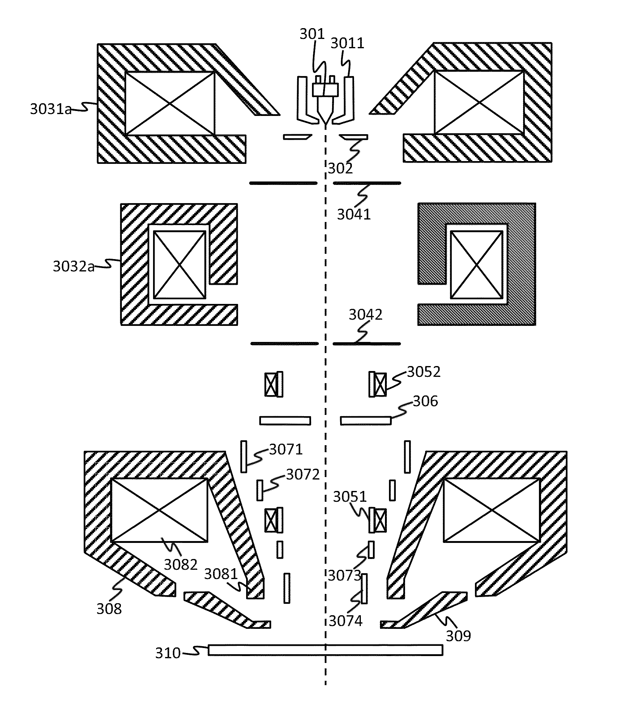
[0034]In one embodiment in FIG. 3(a), the immersion magnetic lens 3031a and the condenser lens 3032a are altered to a double lens with a magnetic immersion condenser lens 3031d and a magnetic non-immersion condenser lens 3032d following the lens 3031d as shown in FIG. 3(d). While operating in the inspection mode, the magnetic immersion condenser lens 3031d is turned on and on the contrast, the magnetic immersion condenser lens 3031d is turned off and the non-magnetic immersion condenser lens 3032d has to be turned on for the review mode of operation. And the two deflection systems 3071 to 3074 and two Wien filters 3051 and 3052 have the same operation with the embodiment shown in FIG. 3(a). Herein, one aperture can be arranged below the double lens for the preferred beam current.

[0035]In another embodiments according to the embodiments in FIGS. 3(a) and (d), a booster (not shown) can be added to each of them, which stretches from the cathode to the SORIL, to accelerate the beam cur...

second embodiment

[0039]In one embodiment in FIG. 5(a), the immersion magnetic lens 503a and the condenser lens 504a are altered to a double lens 503b and 504b as shown in FIG. 5(b). The two working modes of inspection and review have the same operation with the embodiment shown in FIG. 3(d).

[0040]In another embodiments according to the second embodiment in FIGS. 5(a) and (b), a booster (not shown) can be added to each of them, which stretches from the cathode to the stage, to accelerate the beam current. The second Wien filter can be handled as that of the first embodiment.


PUM


Abstract

The present invention provides an improved electron-optical apparatus for the inspection and review of the specimen, and for the defect inspection, an inspection mode of operation is performed to generate inspection data, wherein the large beam current is formed by a magnetic immersion lens to scan the specimen, and preferably the objective lens system, a swing objective retarding immersion lens, focuses the beam current and generates the large scanning field, and for the defect review, the review mode of operation is performed to analyze the defects, wherein the large beam current is abandoned and the small beam current is adopted to examine the specimen without a large scanning field, and in order to properly select and detect signal charged particles excited from the specimen, a first Wien filter is utilized to select the acquired signal particles and a second Wien filter is used to compensate the aberrations induced when the signal particles pass through the first Wien filter.

Description

BACKGROUND OF THE INVENTION[0001]The invention relates to an electron optical inspection apparatus for sample inspection and defect review in semiconductor manufacturing and the like. However, it would be recognized that the invention has a much broader range of applicability.[0002]All the way through, during the fabrication processes of semiconductor devices such as integrated circuits (ICs) and memory devices, the defects inevitably existed on the wafer, even on the reticle or mask, keep impacting the yield of products, and thus the measure regarding to the detection of defects is supremely demanded. Prior to the sub-micron age, the optical inspection tools were the significant means to detect the defects on the wafer. However, with the narrowing dimension of the semiconductor devices, the conventional optical inspection tool was thrown into a dilemma for the dimension of defects became smaller than its optical wavelength to probe defects. On the other hand, with the progress of t...

Claims


Application Information

Patent Timeline
Patent Type & Authority Patents(United States)
IPC IPC(8): H01J37/22H01J37/285H01J37/28H01J37/05
CPCH01J37/222H01J37/05H01J37/28H01J37/285H01J37/04H01J37/265H01J2237/2449H01J2237/2817
Inventor LI, SHUAI
Owner ASML NETHERLANDS BV
Why Eureka
Try Eureka