Method for patterning a substrate for planarization

a technology of substrate and planarization, applied in the direction of semiconductor/solid-state device manufacturing, basic electric elements, electric instruments, etc., can solve the problems of limiting the pitch or spacing between exposed features, conventional patterning techniques suffer from poor resolution or rough surface of etched features, conventional techniques cannot provide a level of uniformity and fidelity, etc., to achieve the effect of improving ler/lwr, improving feature density, and reducing feature siz

Active Publication Date: 2016-09-06
TOKYO ELECTRON LTD
View PDF6 Cites 4 Cited by
  • Summary
  • Abstract
  • Description
  • Claims
  • Application Information

AI Technical Summary

Benefits of technology

[0007]Pitch reduction techniques, often somewhat erroneously termed “pitch multiplication” as exemplified by “pitch doubling” etc., can extend the capabilities of photolithography beyond feature size limitations (optical resolution limitations). That is, conventional multiplication of pitch (more accurately pitch reduction or multiplication of pitch density) by a certain factor involves reducing a target pitch by a specified factor. Double patterning techniques used with 193 nm immersion lithography are conventionally considered as one of the most promising techniques to pattern 22 nm nodes and smaller. Noteworthy is that self-aligned spacer double patterning (SADP) has already been established as a pitch density doubling process and has been adapted in high volume manufacturing of NAND flash memory devices. Moreover, ultra-fine resolution can be obtained to repeat the SADP step twice as pitch quadrupling.
[0009]Techniques disclosed herein, provide a method for pitch reduction (increasing pitch / feature density) for creating high-resolution features. Patterning techniques herein can quadruple a density of features in a given pattern, or dramatically reduce feature size. In other words, such patterning techniques can take an initial critical dimension pitch and reduce this initial pitch so that it is a quarter or less of its initial size. This feature reduction technique also provides features or openings having high uniformity and fidelity.
[0012]The result of this patterning process provides significant improvements in feature size reduction. Using CMP to remove fill material, and by making the top of the conformally applied spacers atomically flat provides dramatic improvement in LER / LWR. This novel technique provides an improved method for increasing the feature density and provides more compact and uniform arrays without harming feature resolution.

Problems solved by technology

Conventional lithographic techniques for exposing a pattern of radiation or light onto a substrate have various challenges that limit a size of features exposed, and limit pitch or spacing between exposed features.
Although there exist several patterning techniques to increase pattern or pitch density, conventional patterning techniques suffer from poor resolution or rough surfaces of etched features.
Thus, conventional techniques cannot provide a level of uniformity and fidelity desired for very small dimensions (20 nm and smaller).

Method used


Image

  • Method for patterning a substrate for planarization
  • Method for patterning a substrate for planarization
  • Method for patterning a substrate for planarization

Examples


Embodiment Construction

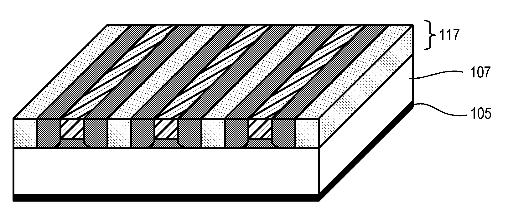
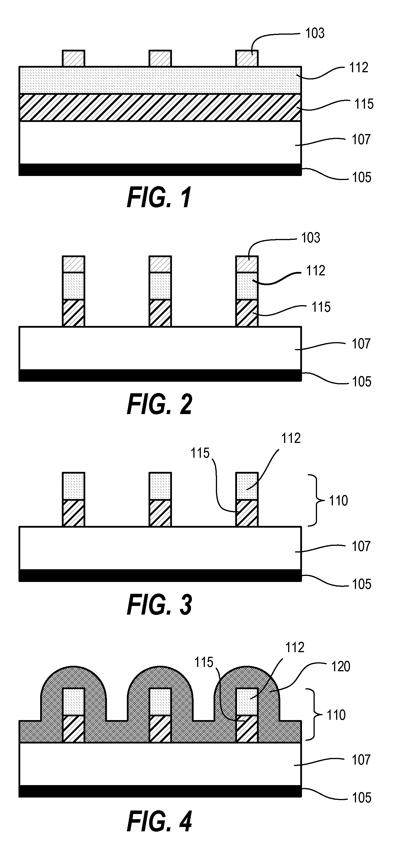
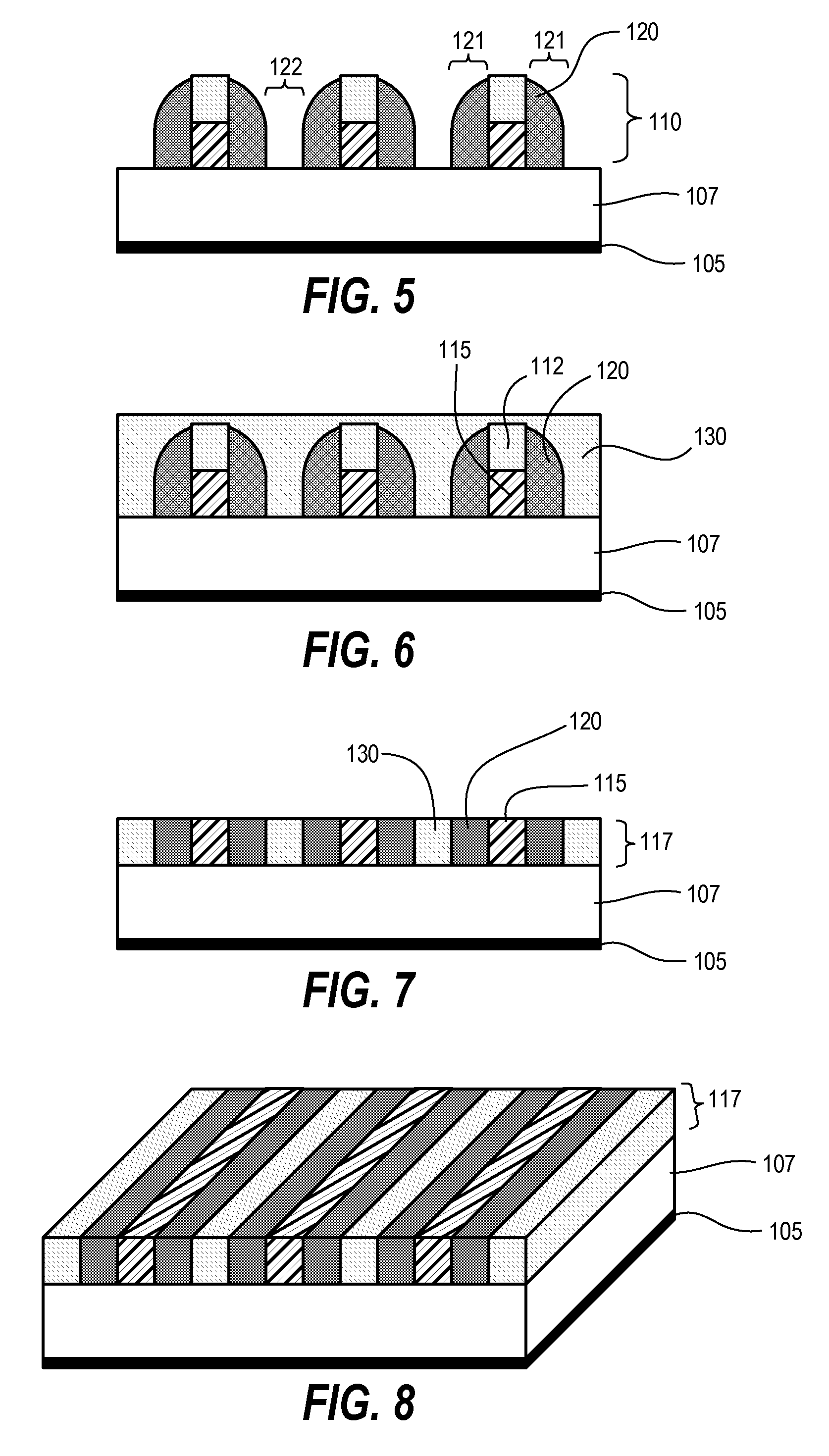
[0025]Techniques disclosed herein include increasing pattern density for creating high-resolution trenches, contact openings, and other features. Patterning techniques herein include combining double patterning techniques, sidewall image techniques, as well as novel planarizing techniques. Patterning techniques herein can quadruple a density of features in a given pattern. In other words, such patterning techniques can take an initial critical dimension pitch and reduce this initial pitch so that it is a quarter or eighth of its initial size, or smaller. This feature reduction technique also provides features or openings having high uniformity and fidelity. Patterning techniques herein can also enable doubled patterns at higher resolutions than is conventionally available.

[0026]In general, methods herein can include depositing a conformal spacer on a bi-layer or tri-layer mandrel (multi-layer) or other topographic feature. The conformal spacer thus wraps around the mandrels and unde...


PUM


Abstract

Techniques disclosed herein include increasing pattern density for creating high-resolution contact openings, slots, trenches, and other features. A conformal spacer is applied on a bi-layer or tri-layer mandrel (multi-layer) or other relief feature. The conformal spacer thus wraps around the mandrels and is also deposited on an underlying layer. A fill material is deposited to fill gaps or spaces between sidewall spacers. A CMP planarization step then removes substrate stack material down to a material interface of the bi-layer or tri-layer mandrel, with a middle or lower material of the mandrel being a CMP-stop material. This technique essentially cuts off or removes rounded features such as upper portions of sidewall spacers, thereby providing a spacer material with a planar top surface that can be uniformly etched and transferred to underlying layers.

Description

CROSS REFERENCE TO RELATED APPLICATIONS[0001]The present application claims the benefit of U.S. Provisional Patent Application No. 61 / 943,486, filed on Feb. 23, 2014, entitled “Method for Patterning a Substrate for Planarization,” which is incorporated herein by reference in its entirety.BACKGROUND OF THE INVENTION[0002]This disclosure relates to substrate processing, and, more particularly, to techniques for patterning substrates including patterning semiconductor wafers.[0003]Methods of shrinking line-widths in lithographic processes have historically involved using greater-NA optics (numerical aperture), shorter exposure wavelengths, or interfacial media other than air (e.g., water immersion). As the resolution of traditional lithographic processes has approached theoretical limits, manufacturers have started to turn to double-patterning (DP) methods to overcome optical limitations.[0004]In material processing methodologies (such as photolithography), creating patterned layers co...

Claims


Application Information

Patent Timeline
Patent Type & Authority Patents(United States)
IPC IPC(8): H01L21/302H01L21/3105H01L21/02H01L21/311H01L21/033
CPCH01L21/31055H01L21/0228H01L21/0337H01L21/31111H01L21/02266
Inventor DEVILLIERS, ANTON J.
Owner TOKYO ELECTRON LTD
Why Eureka
Try Eureka