Semiconductor package with coated side walls and method of manufacture

a semiconductor and side wall technology, applied in the direction of coatings, microstructure devices, microstructure technology, etc., can solve the problems of contamination and unsuitable particles during device dicing, and achieve the effects of increasing the adhesion of the coating material, and reducing the risk of contamination

Active Publication Date: 2016-09-06
SENSIRION AG
View PDF8 Cites 0 Cited by
  • Summary
  • Abstract
  • Description
  • Claims
  • Application Information

AI Technical Summary

Benefits of technology

[0013]In a preferred embodiment, the coating material seals the cut surface to reduce emission of particles related to a dicing process used to manufacture the cut surface and / or seals the cut surface to protect it.
[0020]In one embodiment, at least one gap extends in a direction perpendicular to the side wall and is filled by a portion of the coating material. A gap in a side wall may for example arise in adhesive bonding of a silicon chip and a silicon cap. Filling the gap may serve to confine remains of dicing slurry and / or to protect the edges of a gap and / or the adhesive material which might be more sensitive to mechanical and chemical impact.
[0022]In another embodiment, the front end of the coating material coated on at least one of the side walls is covered by a lateral extension of the front side material A or by a lateral extension of the back side material B. This may serve to increase adhesion of the coating material and / or to hide it from view and / or to protect it from wear.

Problems solved by technology

When a semiconductor device is packaged, especially in a batch process, undesired particles may arise during device dicing, e.g. by sawing or laser cutting.
In such a process, contamination may arise in form of particles released from the cut surfaces or there may be thermal impact arising from the laser cutting step.

Method used


Image

  • Semiconductor package with coated side walls and method of manufacture
  • Semiconductor package with coated side walls and method of manufacture
  • Semiconductor package with coated side walls and method of manufacture

Examples


Embodiment Construction

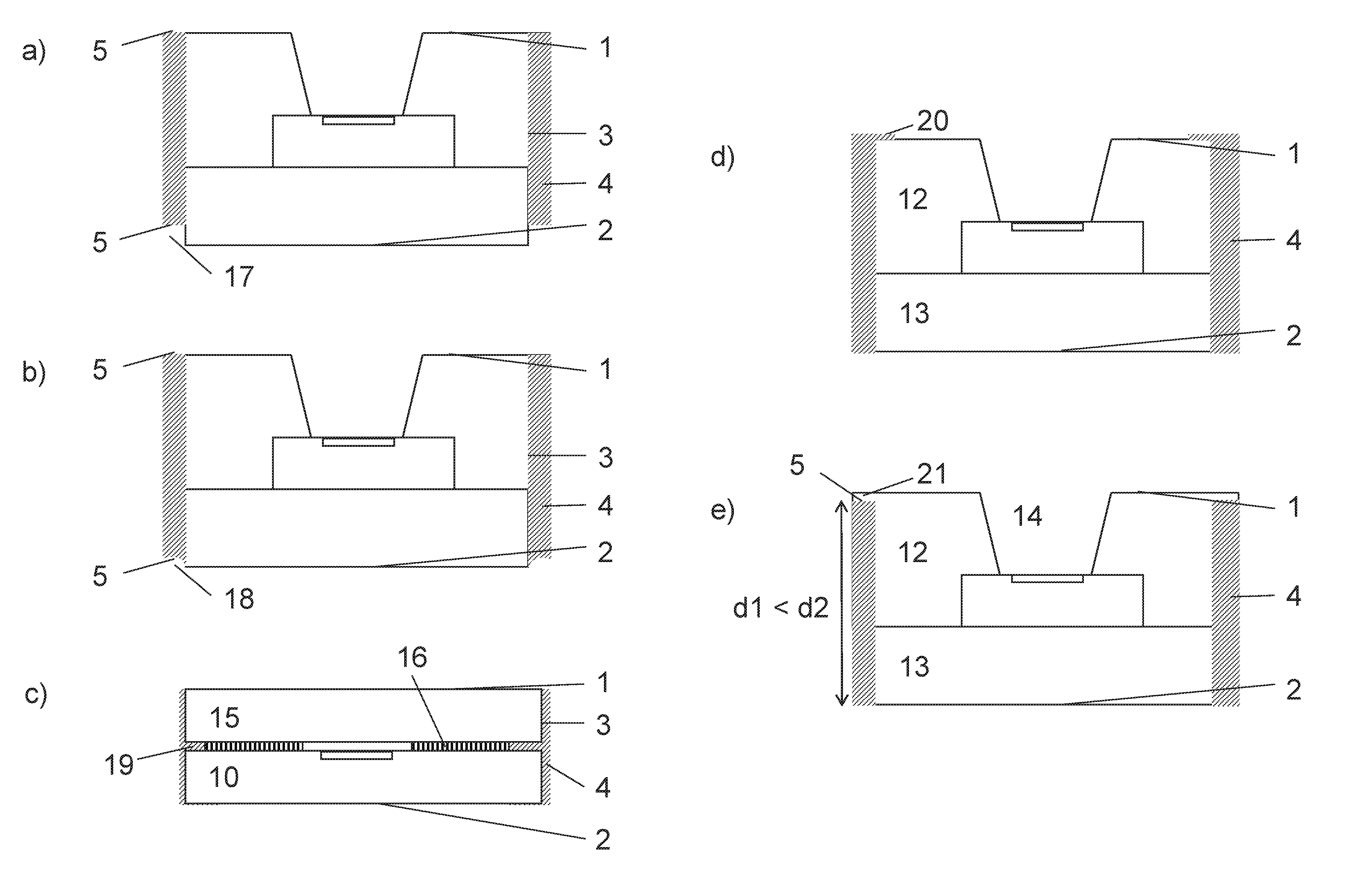
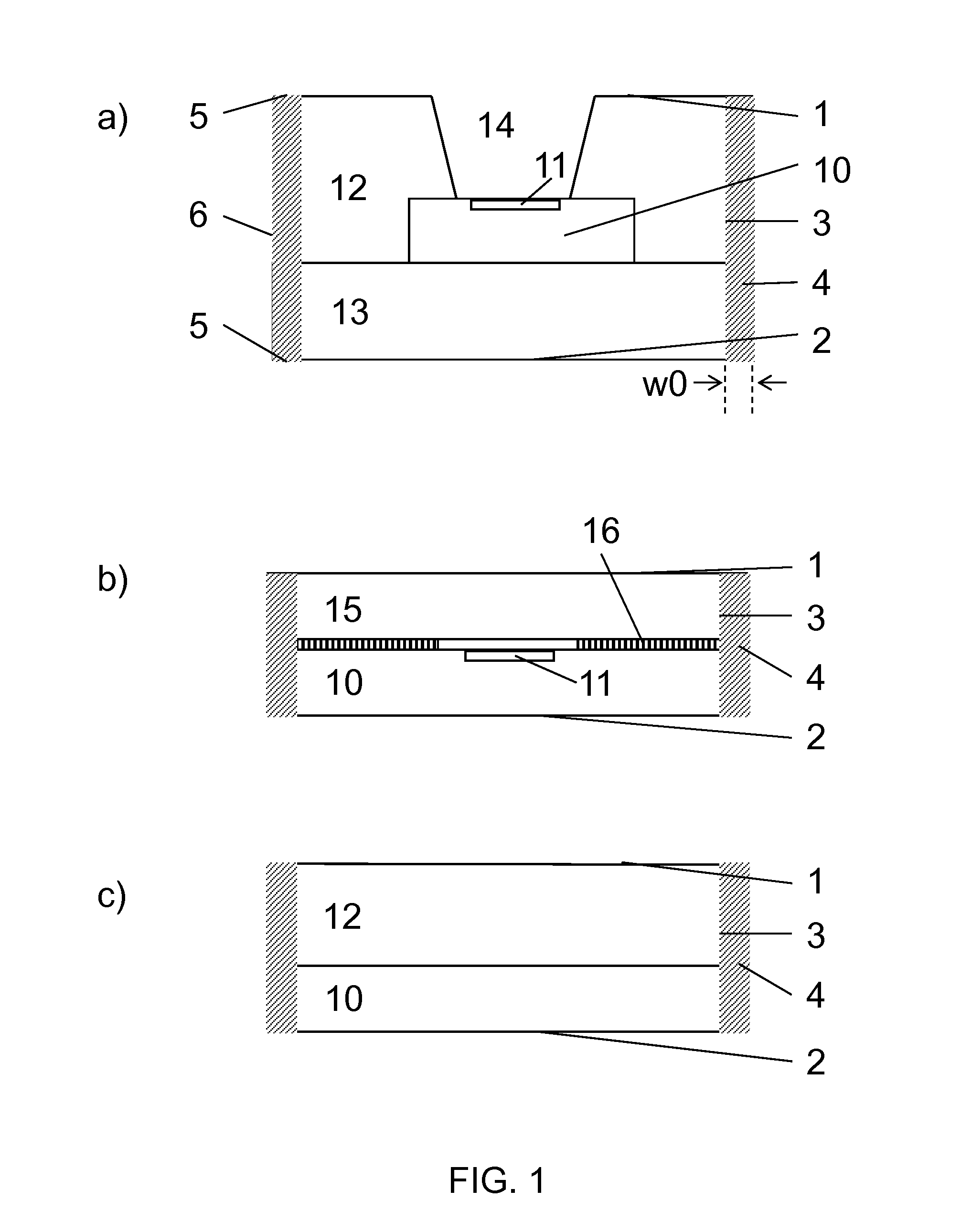
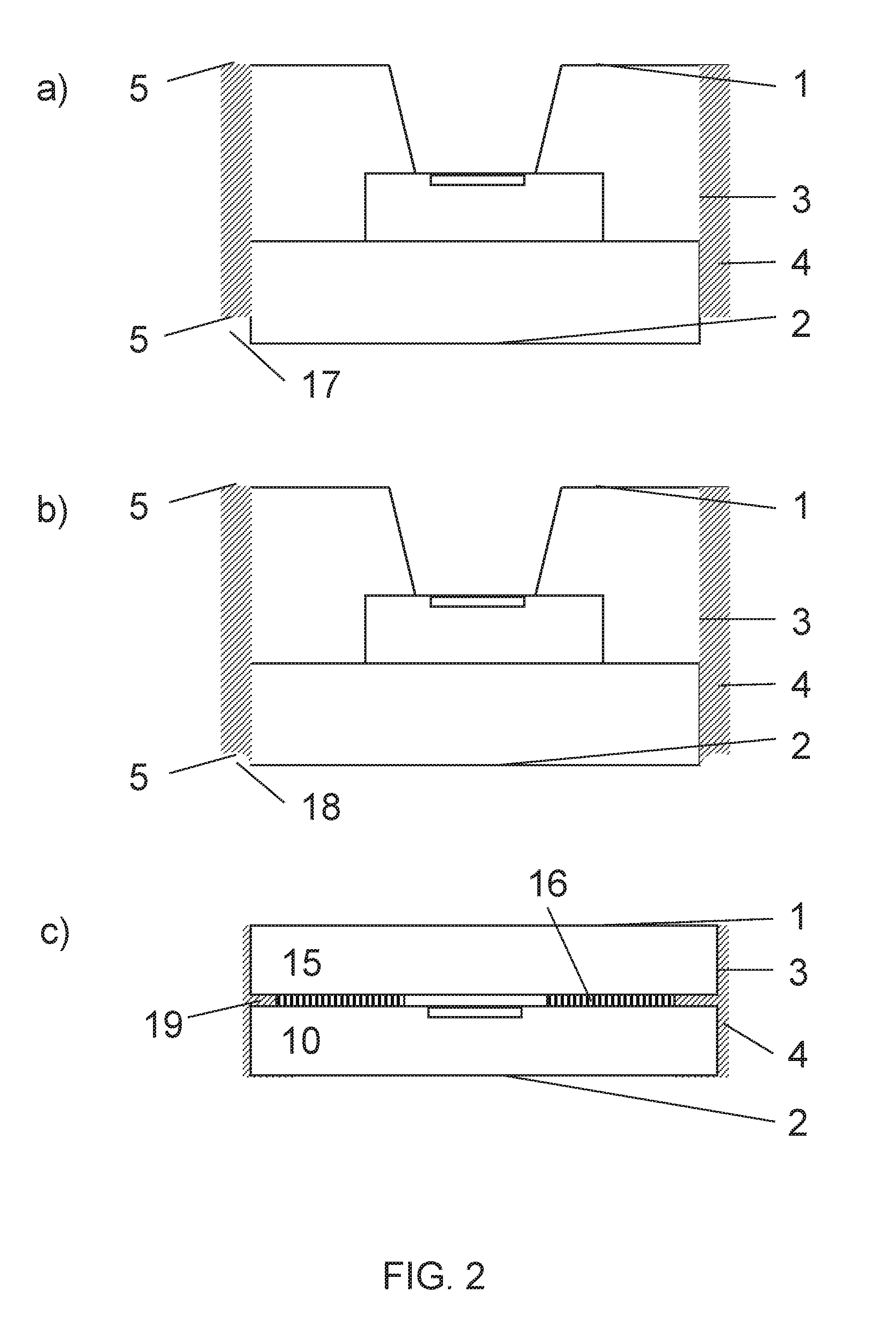
[0045]FIG. 1a) shows a schematic sectional view of a semiconductor package in accordance with an embodiment of the present invention. The semiconductor package has a front side 1 and back side 2.

[0046]In this embodiment, a silicon die 10 which includes a sensitive element 11 is attached to a support 13. The silicon die 10 may include features such as an integrated processing circuit and / or a suspended membrane and / or a heater structure. The support 13 may comprise means for external electrical contacting, e.g. one of a printed circuit board, a ceramic support or a lead frame. In this embodiment, the semiconductor package comprises a mold 12 which has an access opening 14 from the front side 1 to the sensitive element 11. If the means for external electrical contacting is a lead frame, the lead frame may also be partially packaged in the mold.

[0047]In this embodiment, the semiconductor package has side walls 3 which are coated completely between front side 1 and back side 2 with a co...


PUM

PropertyMeasurementUnit
widthaaaaaaaaaa
width w0aaaaaaaaaa
width w1aaaaaaaaaa

Abstract

A semiconductor package including an integrated device, the package having a front side, a back side and side walls linking the front and back sides, wherein each side wall is coated, to at least 80% of its area, with a coating material different from the material(s) of the back and front sides. A method of manufacturing a semiconductor package by providing an assembly containing an array of the packages, the assembly having thickness d0 and being attached to a dicing tape of thickness dd, fabricating a set of first dicing streets with width w1 and depth d1<(d0+dd), filling the first dicing streets at least partially with a coating material, and fabricating, in the coating material in each first dicing street, a second dicing street with width w2≦w1 and depth d2≧d0 but <(d0+dd).

Description

CROSS REFERENCE TO RELATED APPLICATIONS[0001]This application claims priority of European Patent Application 14167397.0, filed May 7, 2014, the contents of which is incorporated herein by reference in its entirety.FIELD OF THE INVENTION[0002]The present invention relates to a semiconductor package and a method for manufacturing a semiconductor package.BACKGROUND OF THE INVENTION[0003]When a semiconductor device is packaged, especially in a batch process, undesired particles may arise during device dicing, e.g. by sawing or laser cutting.[0004]In KR100395754 B1 for example, a pre-cutting process is performed by cutting particular units of a semiconductor package. The particular units of the semiconductor package are cut by using a dicing wheel. A cleaning and a drying process is performed to clean cut sludge caused by the pre-cutting process. A laser beam cutting process is performed by cutting the remaining thickness of the semiconductor package.[0005]In such a process, contaminatio...

Claims


Application Information

Patent Timeline
Patent Type & Authority Patents(United States)
IPC IPC(8): H01L23/31H01L21/302H01L21/56B81C1/00H01L23/29
CPCH01L23/3185B81C1/00261B81C1/00777H01L21/302H01L21/561H01L23/293H01L2924/0002H01L2924/00B81B7/0016B81C1/00896
Inventor HUNZIKER, WERNER
Owner SENSIRION AG
Why Eureka
Try Eureka