
Three dimensional (3D) memory including error detection circuitry

a three-dimensional memory and error detection technology, applied in error detection/correction, redundant data error correction, instruments, etc., can solve the problems of reducing the read/write throughput of the data storage device, reducing power consumption, and displaying errors on the data storage device. , to achieve the effect of reducing bus traffic and high data traffi

Active Publication Date: 2016-09-13
SANDISK TECH LLC
View PDF24 Cites 3 Cited by
  • Summary
  • Abstract
  • Description
  • Claims
  • Application Information

AI Technical Summary

Benefits of technology

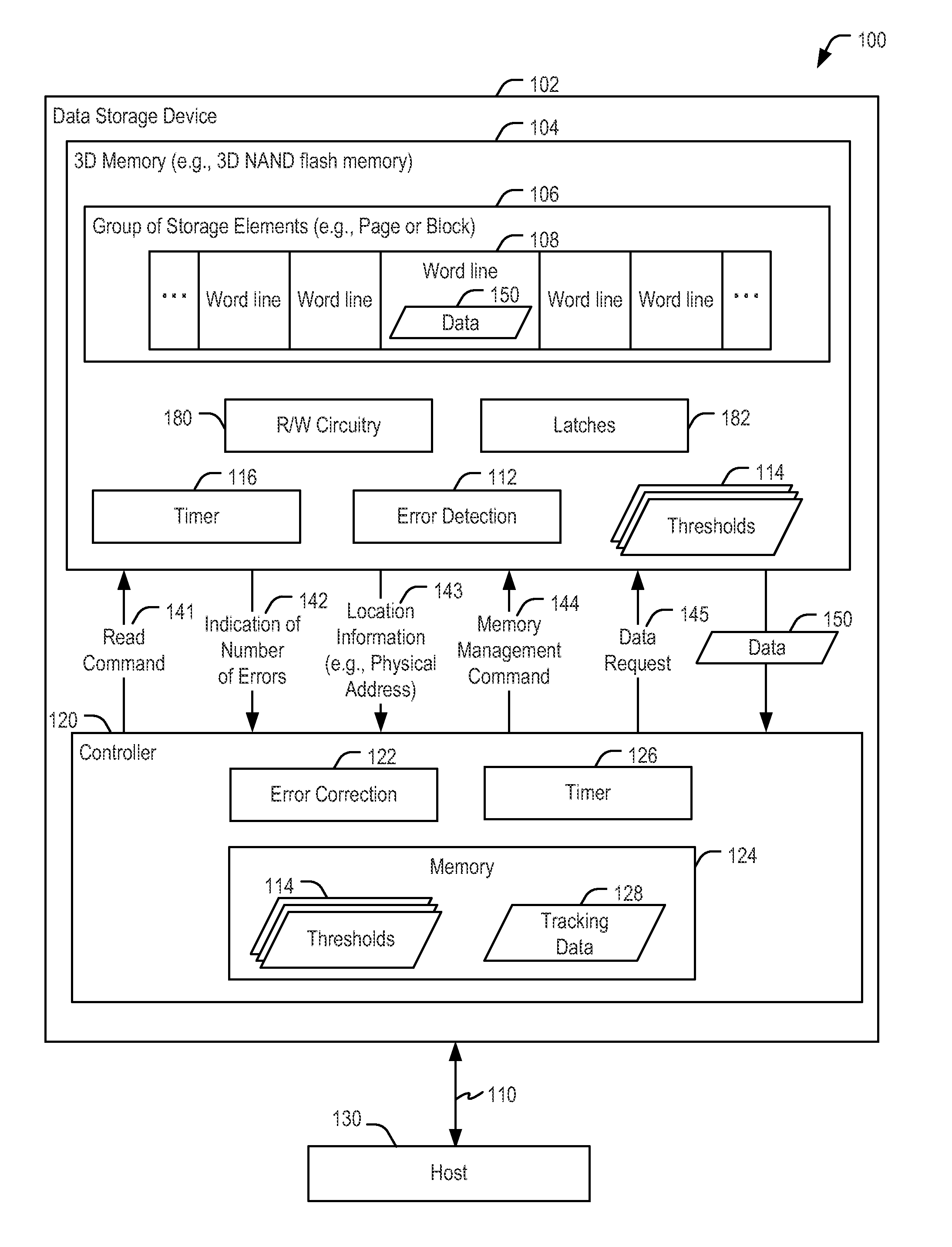
The patent is about a data storage device that includes a controller and a non-volatile memory. The non-volatile memory has error detection circuitry, which can detect errors while reading data from the memory without sending the data to the controller via the bus. This reduces bus traffic associated with error detection. The device can also use multiple error correction codes to further decrease the amount of data traffic. The technical effect of this patent is to improve the speed and efficiency of data storage and retrieval.

Problems solved by technology

Due to manufacturing defects and / or wear and tear, a data storage device may exhibit errors.
Transmission of data from the memory to the controller for error detection and other memory management operations may increase traffic on the bus, which may reduce read / write throughput of the data storage device.
Improved reliability may enable operation using a less powerful ECC engine, may result in reduced power consumption, may result in reduced device size, may result in reduced manufacturing cost, or any combination thereof.

Method used


Image

  • Three dimensional (3D) memory including error detection circuitry
  • Three dimensional (3D) memory including error detection circuitry
  • Three dimensional (3D) memory including error detection circuitry

Examples


Embodiment Construction

[0012]Particular embodiments of the present disclosure are described with reference to the drawings. In the description, common features are designated by common reference numbers throughout the drawings.

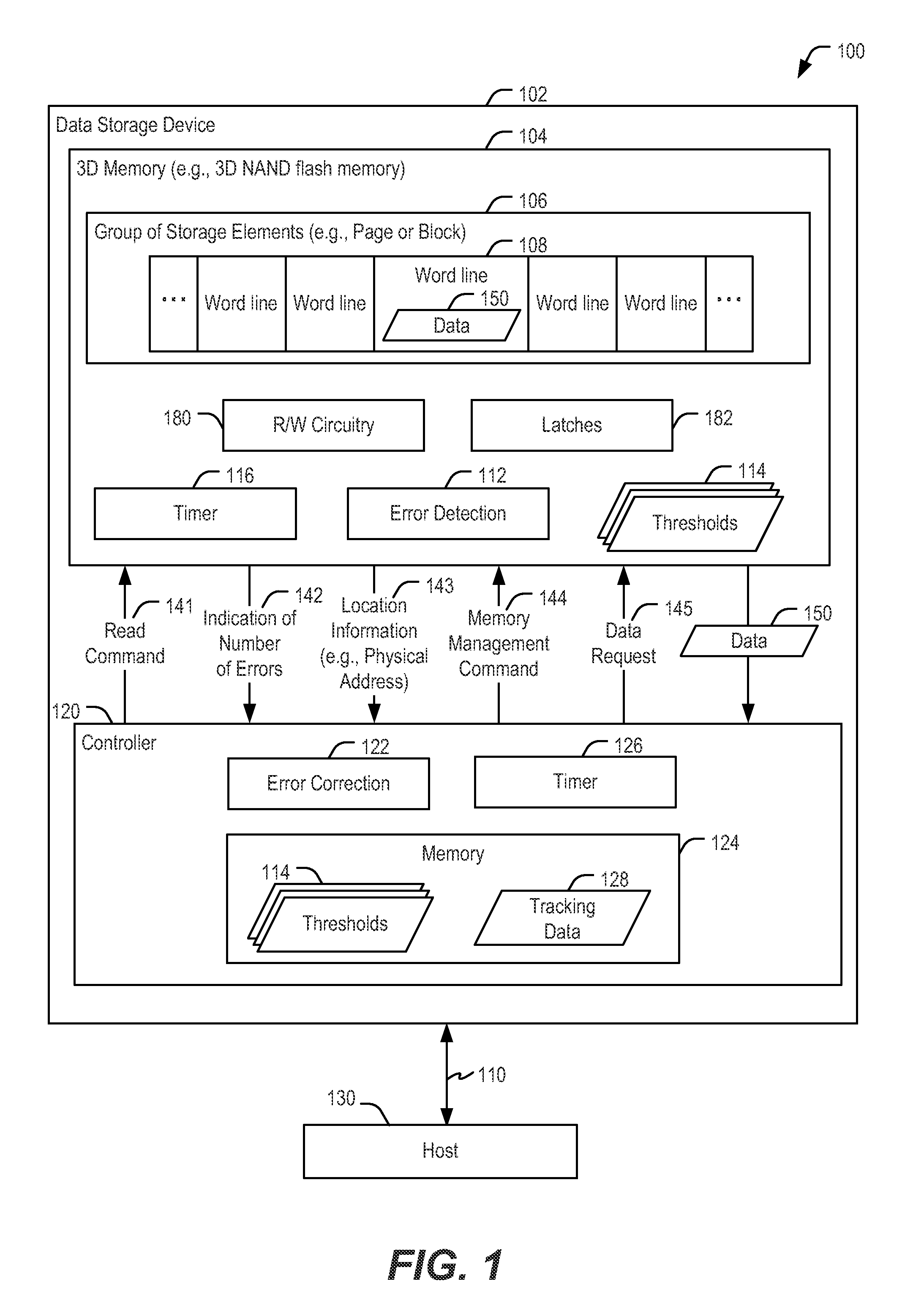
[0013]Referring to FIG. 1, a particular embodiment of a system 100 includes a data storage device 102 coupled to a host device 130 via a host interface 110. The data storage device 102 includes a three-dimensional (3D) memory 104, where the 3D memory 104 includes error detection circuitry 112.

[0014]The host device 130 may be configured to provide data (e.g., user data) to be stored at the 3D memory 104 or to request data to be read from the 3D memory 104. For example, the host device 130 may include a mobile telephone, a music player, a video player, a gaming console, an electronic book reader, a personal digital assistant (PDA), a computer, such as a laptop computer or notebook computer, any other electronic device, or any combination thereof. The host device 130 communicates via a...


PUM


Abstract

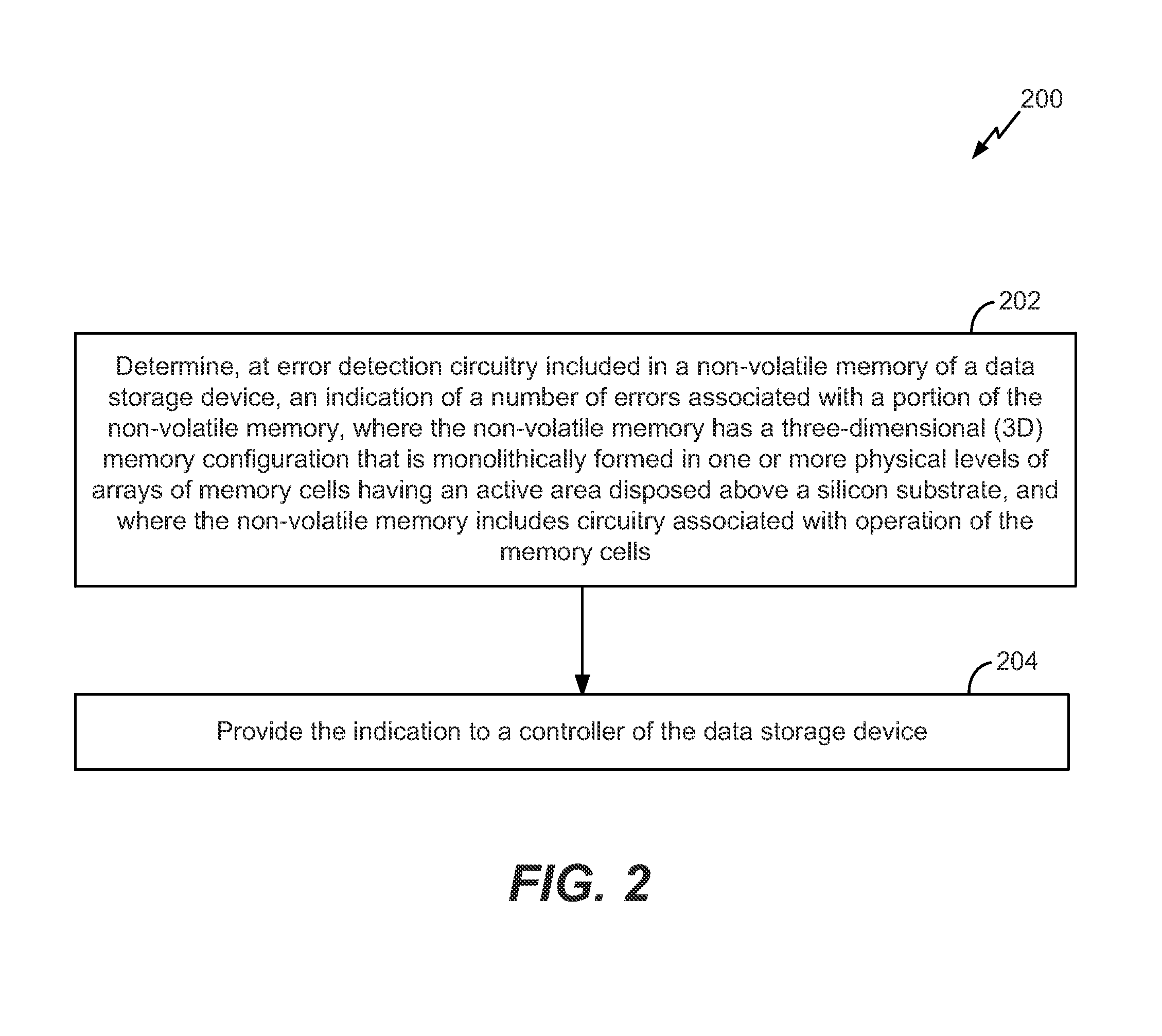
A method performed at a non-volatile memory of a data storage device includes determining, at error detection circuitry included in the non-volatile memory, an indication of a number of errors associated with a portion of the non-volatile memory. The method also includes providing the indication to a controller of the data storage device, where the controller includes error correction circuitry. The non-volatile memory has a 3D configuration that is monolithically formed in one or more physical levels of arrays of memory cells having an active area disposed above a silicon substrate. The non-volatile memory includes circuitry associated with operation of the memory cells.

Description

FIELD OF THE DISCLOSURE[0001]The present disclosure is generally related to a three dimensional (3D) memory that includes error detection circuitry.BACKGROUND[0002]Non-volatile data storage devices, such as embedded memory devices (e.g., embedded MultiMedia Card (eMMC) devices) and removable memory devices (e.g., removable universal serial bus (USB) flash memory devices and other removable storage cards), have allowed for increased portability of data and software applications. Users of non-volatile data storage devices increasingly rely on the non-volatile storage devices to store and provide rapid access to a large amount of data.[0003]Due to manufacturing defects and / or wear and tear, a data storage device may exhibit errors. The data storage device may be capable of performing error correction to correct certain types of errors. To perform error correction and other memory management operations, data may be read from a memory on a first chip / die and provided to a controller on a...

Claims


Application Information

Patent Timeline
Patent Type & Authority Patents(United States)
IPC IPC(8): G06F11/00G06F11/07G06F11/10
CPCG06F11/076G06F11/1048G06F11/1068G06F11/0751
Inventor D'ABREU, MANUEL ANTONIO
Owner SANDISK TECH LLC
Learn More