Printed circuit board and power supply unit
a technology of power supply unit and printed circuit board, which is applied in the direction of printed circuit, printed circuit components, printed circuit non-printed electric components association, etc., can solve the problems of reducing the tightening force of the screw, lowering the reliability of connection, etc., and achieves the effect of reducing design constraints and ensuring reliability
- Summary
- Abstract
- Description
- Claims
- Application Information
AI Technical Summary
Benefits of technology
Problems solved by technology
Method used
Image
Examples
embodiment 1
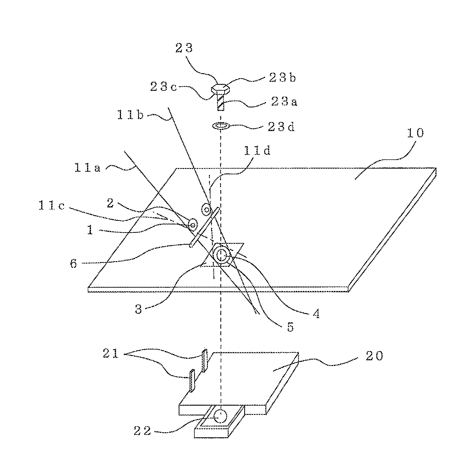
[0017]FIG. 1 is a schematic view of a printed circuit board 10 according to Embodiment 1 of the present invention.
[0018]The printed circuit board 10 has a wiring pattern made of conductive copper foil or the like (not shown in FIG. 1) printed on one or two surfaces of an insulated substrate having electric insulation property, and is used as a power supply unit when a power module 20 including an integrated circuit such as thyristor, power MOSFET and IGBT is mounted.
[0019]The power module 20 includes a plurality of lead terminals 21 and one or a plurality of screw terminals 22.
[0020]A plurality of through holes 1 and an electrode section 3 are formed on the printed circuit board 10. The plurality of through holes 1 are arrayed to receive the lead terminals 21 of the power module 20, and connect them to the printed circuit board 10 by soldering. The electrode section 3 has a through hole for fastening a screw 23 to the screw terminal 22 of the power module 20 to electrically connect ...
embodiment 2
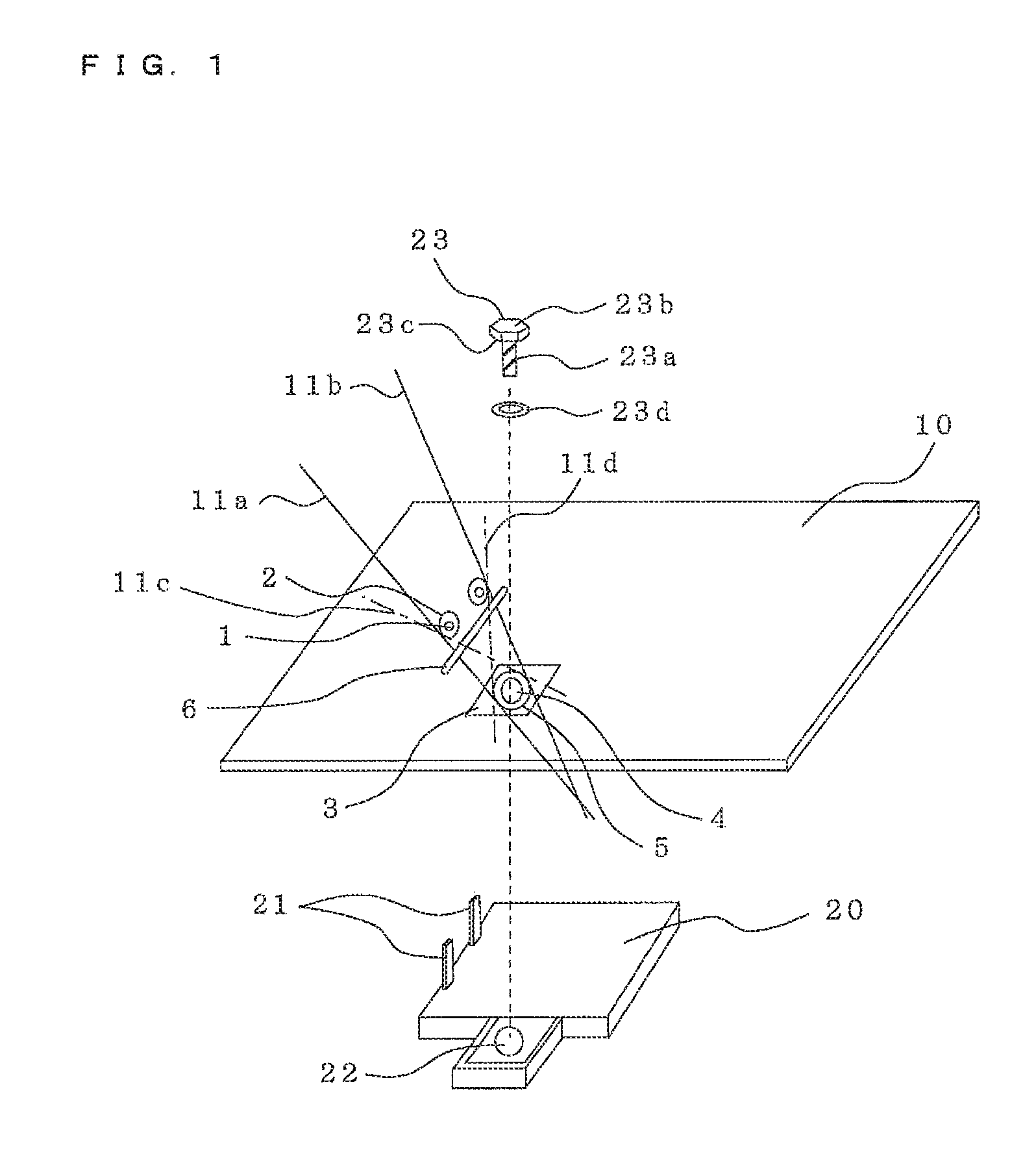
[0031]FIG. 2 is a schematic view of the printed circuit board 10 according to Embodiment 2 of the present invention.
[0032]In Embodiment 1, two ends of the groove 6 extend from respective common tangents 11. This prevents stress from concentrating on the solder connection area of the lead terminals 21 of the power module 20 in screwing of the power module 20.
[0033]Embodiment 2 defines an amount of extension 7 of the groove 6. That is, the screw hole 4 in the electrode section 3 of the printed circuit board 10 generally has a diameter larger than that of the screw 23, and the contact area of the printed circuit board 10 and the screw 23 is displaced by an amount corresponding to the clearance between the screw 23 and the screw hole 4.
[0034]Accordingly, letting D be the inner diameter of the screw hole 4, and d be the outer diameter of the screw 23 (the outer diameter of the external thread 23a), the groove 6 is formed so as to extend from each common tangent 11 by an amount correspond...
embodiment 3
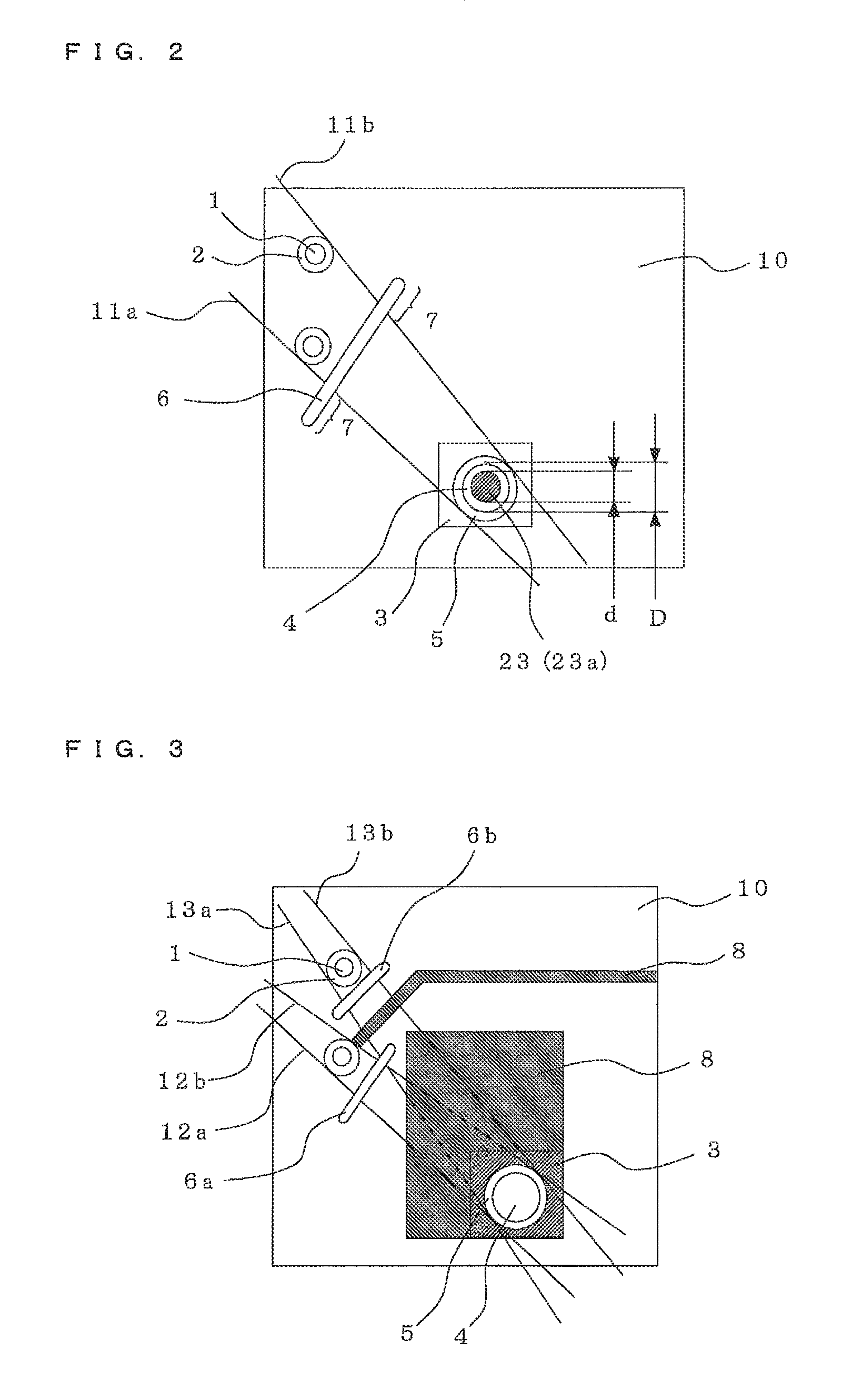
[0036]FIG. 3 is a schematic view of the printed circuit board 10 according to Embodiment 3 of the present invention.
[0037]Embodiments are not limited to a single groove 6. In the case where the groove 6 cannot be provided due to factors associated with the wiring pattern 8 located in the surrounding area, grooves 6a and 6b are individually provided to the through holes 1, as shown in FIG. 3. In this case as well, the groove 6a is provided so as to intersect with two common tangents (non-crossing type common tangents or crossing type common tangents) 12a and 12b, while the groove 6b is formed so as to intersect with two common tangents (non-crossing type common tangents or crossing type common tangents) 13a and 13b.
[0038]In Embodiment 3, since the grooves 6a and 6b are individually provided to the through holes 1, stress acting on the solder connection area of the individual lead terminals 21 can be reduced. Further, since the grooves 6a and 6b can be provided in an area other than ...
PUM
 Abstract
Description
Claims
Application Information


