Printed circuit board and power supply unit

a technology of power supply unit and printed circuit board, which is applied in the direction of printed circuit stress/warp reduction, printed circuit non-printed electric components association, electrical apparatus construction details, etc., can solve the problems of lowering the reliability of connection and reducing the tightening force of screw, so as to ensure reliability and reduce design constraints

Active Publication Date: 2015-09-24
MITSUBISHI ELECTRIC CORP
View PDF2 Cites 4 Cited by
  • Summary
  • Abstract
  • Description
  • Claims
  • Application Information

AI Technical Summary

Benefits of technology

[0009]In the printed circuit board according to the present invention, since the groove is formed between the electrode section and the through hole so as to intersect with two common tangents each of which connects an outer periphery of a contact area of the electrode section being in contact with a head bearing surface of a screw or a washer and an outer periphery of a land of the through hole, stress generated upon screwing of the power module and applied to the solder connection area of the lead terminals can be decreased.
[0010]Accordingly, the present invention can provide the printed circuit board in which when the power module which requires conduction by both the lead terminals and the screw terminal is mounted on the printed circuit board, stress does not act on the solder connection area, reliability can be ensured for a long period of time, and constraints in design can be reduced.

Problems solved by technology

In mounting such a power module on the printed circuit board, when a terminal for screwing (to be referred to as a screw terminal hereinafter) is screwed after the lead terminal is soldered, a crack or the like may occur due to stress generated upon screwing and applied to the solder connection area of the lead terminal, thus lowering the connection reliability.
Further, when the lead terminal is soldered after the screw terminal is screwed, the tightening force of the screw is decreased due to heat generated upon soldering, and retightening of the screw is necessary.

Method used


Image

  • Printed circuit board and power supply unit
  • Printed circuit board and power supply unit
  • Printed circuit board and power supply unit

Examples


embodiment 1

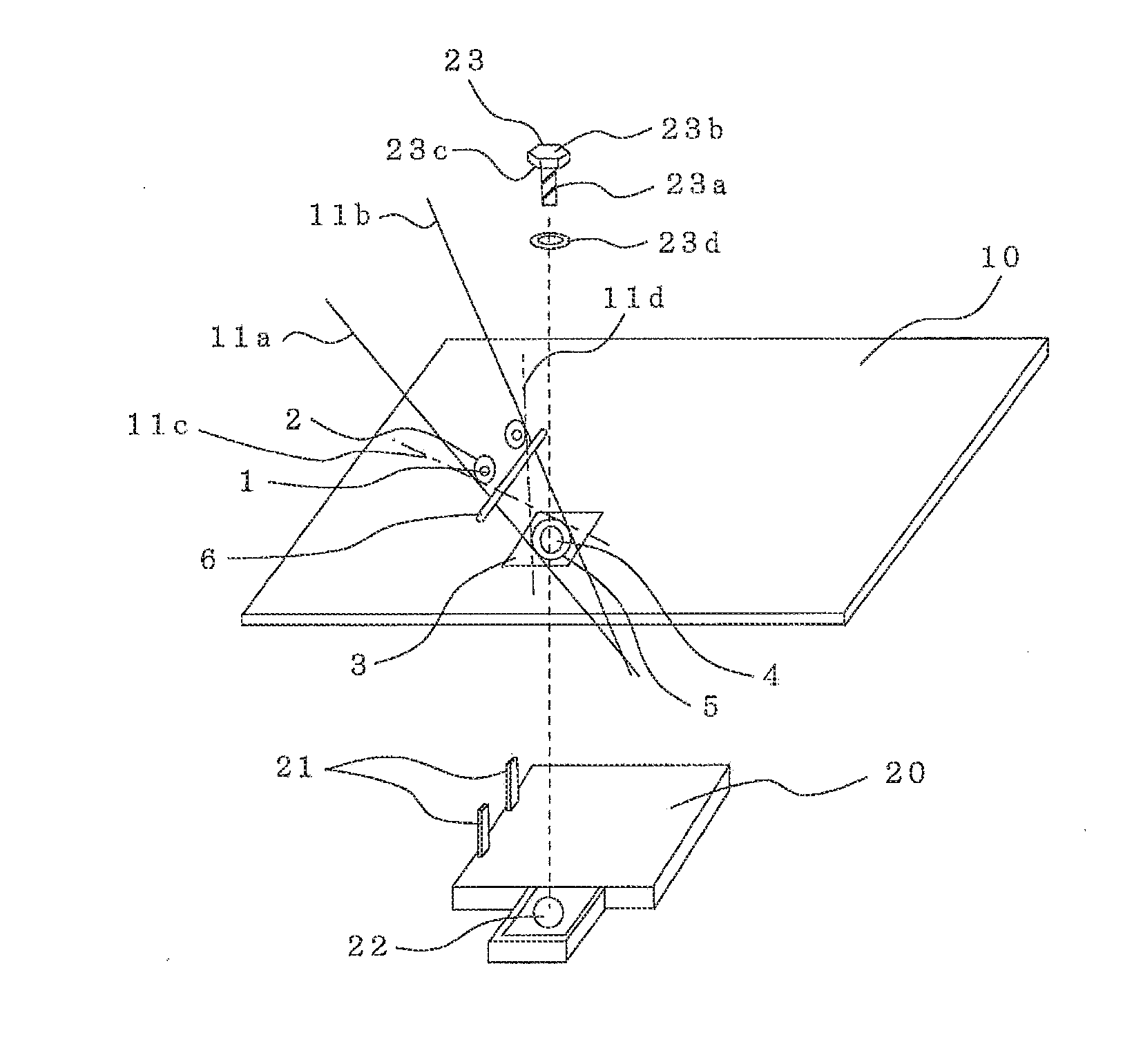
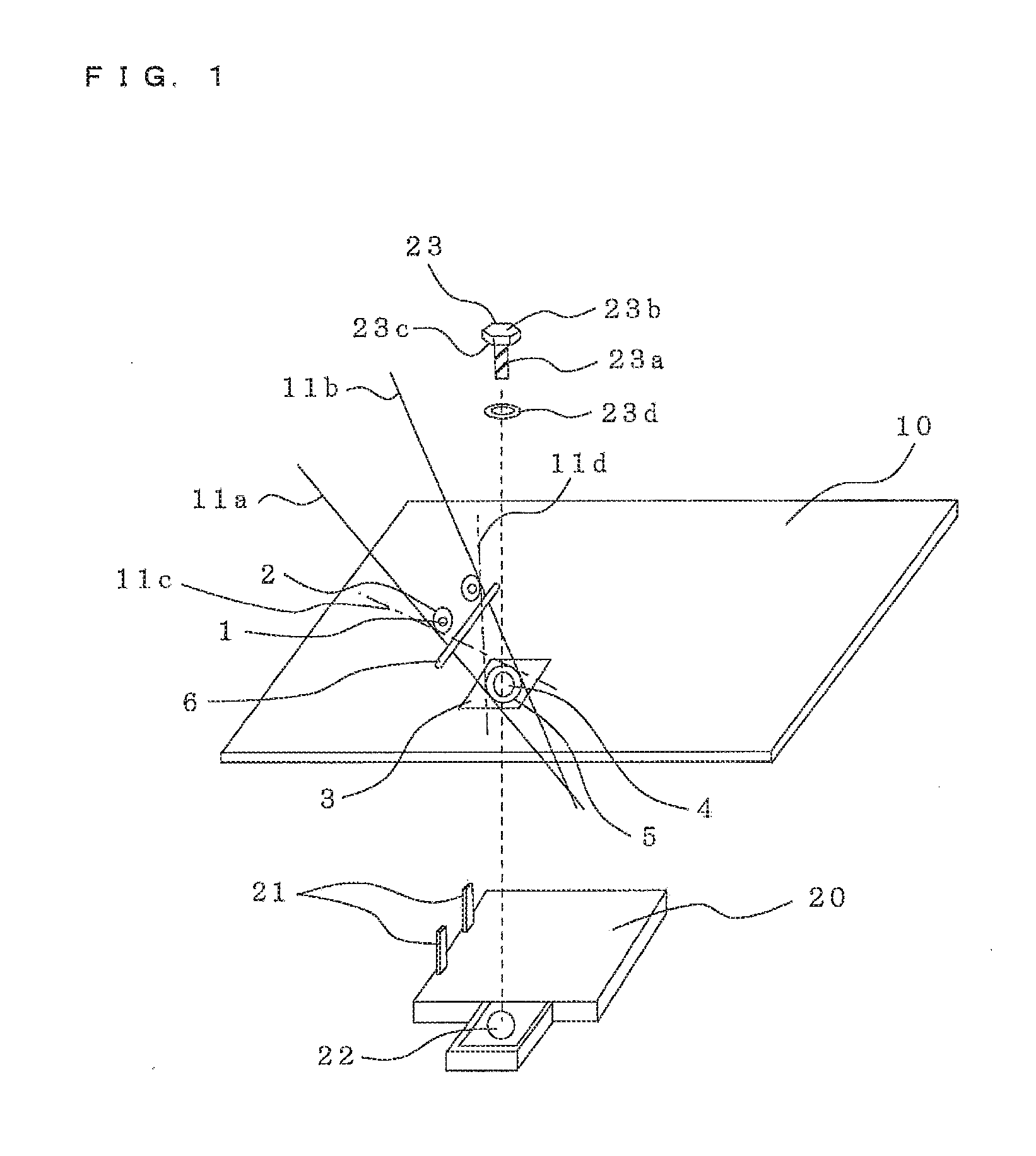
[0016]FIG. 1 is a schematic view of a printed circuit board 10 according to Embodiment 1 of the present invention.

[0017]The printed circuit board 10 has a wiring pattern made of conductive copper foil or the like (not shown in FIG. 1) printed on one or two surfaces of an insulated substrate having electric insulation property, and is used as a power supply unit when a power module 20 including an integrated circuit such as thyristor, power MOSFET and IGBT is mounted.

[0018]The power module 20 includes a plurality of lead terminals 21 and one or a plurality of screw terminals 22.

[0019]A plurality of through holes 1 and an electrode section 3 are formed on the printed circuit board 10. The plurality of through holes 1 are arrayed to receive the lead terminals 21 of the power module 20, and connect them to the printed circuit board 10 by soldering. The electrode section 3 has a through hole for fastening a screw 23 to the screw terminal 22 of the power module 20 to electrically connect ...

embodiment 2

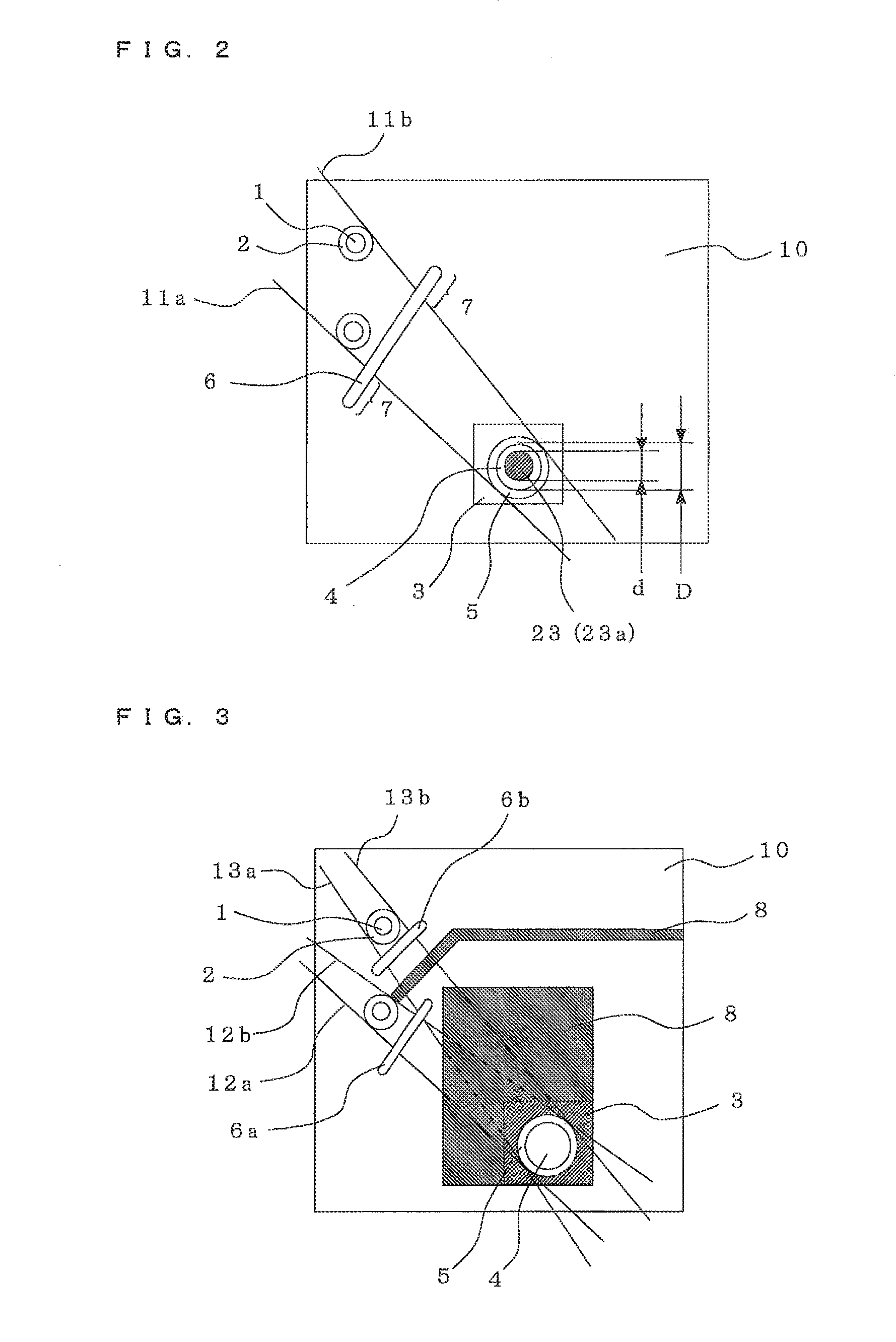
[0030]FIG. 2 is a schematic view of the printed circuit board 10 according to Embodiment 2 of the present invention.

[0031]In Embodiment 1, two ends of the groove 6 extend from respective common tangents 11. This prevents stress from concentrating on the solder connection area of the lead terminals 21 of the power module 20 in screwing of the power module 20.

[0032]Embodiment 2 defines an amount of extension 7 of the groove 6. That is, the screw hole 4 in the electrode section 3 of the printed circuit board 10 generally has a diameter larger than that of the screw 23, and the contact area of the printed circuit board 10 and the screw 23 is displaced by an amount corresponding to the clearance between the screw 23 and the screw hole 4.

[0033]Accordingly, letting D be the inner diameter of the screw hole 4, and d be the outer diameter of the screw 23 (the outer diameter of the external thread 23a), the groove 6 is formed so as to extend from each common tangent 11 by an amount correspond...

embodiment 3

[0035]FIG. 3 is a schematic view of the printed circuit board 10 according to Embodiment 3 of the present invention.

[0036]Embodiments are not limited to a single groove 6. In the case where the groove 6 cannot be provided due to factors associated with the wiring pattern 8 located in the surrounding area, grooves 6a and 6b are individually provided to the through holes 1, as shown in FIG. 3. In this case as well, the groove 6a is provided so as to intersect with two common tangents (non-crossing type common tangents or crossing type common tangents) 12a and 12b, while the groove 6b is formed so as to intersect with two common tangents (non-crossing type common tangents or crossing type common tangents) 13a and 13b.

[0037]In Embodiment 3, since the grooves 6a and 6b are individually provided to the through holes 1, stress acting on the solder connection area of the individual lead terminals 21 can be reduced. Further, since the grooves 6a and 6b can be provided in an area other than ...


PUM


Abstract

A printed circuit board mounted with a power module having both a plurality of lead terminals for soldering and at least one screw terminal for screwing includes a through hole which receives the lead terminal and is soldered to the lead terminal, and an electrode section provided with a screw hole fastened to the screw terminal via a screw. A groove is formed between the electrode section and the through hole so as to intersect with two common tangents each connecting, to an outer periphery of a land of the through hole, an outer periphery of a contact area of the electrode section which is in contact with a head bearing surface of a screw or a washer.

Description

TECHNICAL FIELD[0001]The present invention relates to a printed circuit board and a power supply unit having a power module mounted on the printed circuit board and, more specifically, to a printed circuit board mounted with a power module having both a lead terminal and a screw terminal in a conduction area.BACKGROUND ART[0002]In general, when a power module is mounted on a printed circuit board, a lead terminal of the power module is inserted into a through hole formed in the printed circuit board, and is soldered to electrically connect the power module to the printed circuit board. However, since a large electric current flows through a terminal of, for example, a power supply in a large-capacity power module, a terminal for screwing which has a large area of contact with the printed circuit board is used instead of soldering the lead terminal. Further, even in a large-capacity power module, a lead terminal is used for a terminal of a signal wire or the like in which a small ele...

Claims


Application Information

Patent Timeline
Patent Type & Authority Applications(United States)
IPC IPC(8): H05K1/18H05K1/11
CPCH05K1/116H05K1/18H05K1/0271H05K3/3447H05K2201/09063H05K2201/10409H05K2201/10969H05K2201/10166H05K2201/10659H05K2201/10757
Inventor KAWABATA, RYOHEITAKARABE, YUICHIRO
Owner MITSUBISHI ELECTRIC CORP
Why Eureka
Try Eureka