Semiconductor memory device

a memory device and semiconductor technology, applied in the field of semiconductor memory devices, can solve problems such as retaining data, and achieve the effect of improving the threshold voltage distribution of memory cells

Active Publication Date: 2016-10-18
SK HYNIX INC
View PDF8 Cites 4 Cited by
  • Summary
  • Abstract
  • Description
  • Claims
  • Application Information

AI Technical Summary

Benefits of technology

[0008]Various embodiments are directed to a semiconductor memory device capable of improving a threshold voltage distribution of memory cells by preventing electrons from being trapped in a channel of an unselected memory block during a program operation of the semiconductor memory device.

Problems solved by technology

Volatile memory devices such as Static Random Access memory (SRAM), Dynamic RAM (DRAM) and Synchronous DRAM (SDRAM) do not retain data stored therein when power supply to the device is turned off.

Method used


Image

  • Semiconductor memory device
  • Semiconductor memory device
  • Semiconductor memory device

Examples


Embodiment Construction

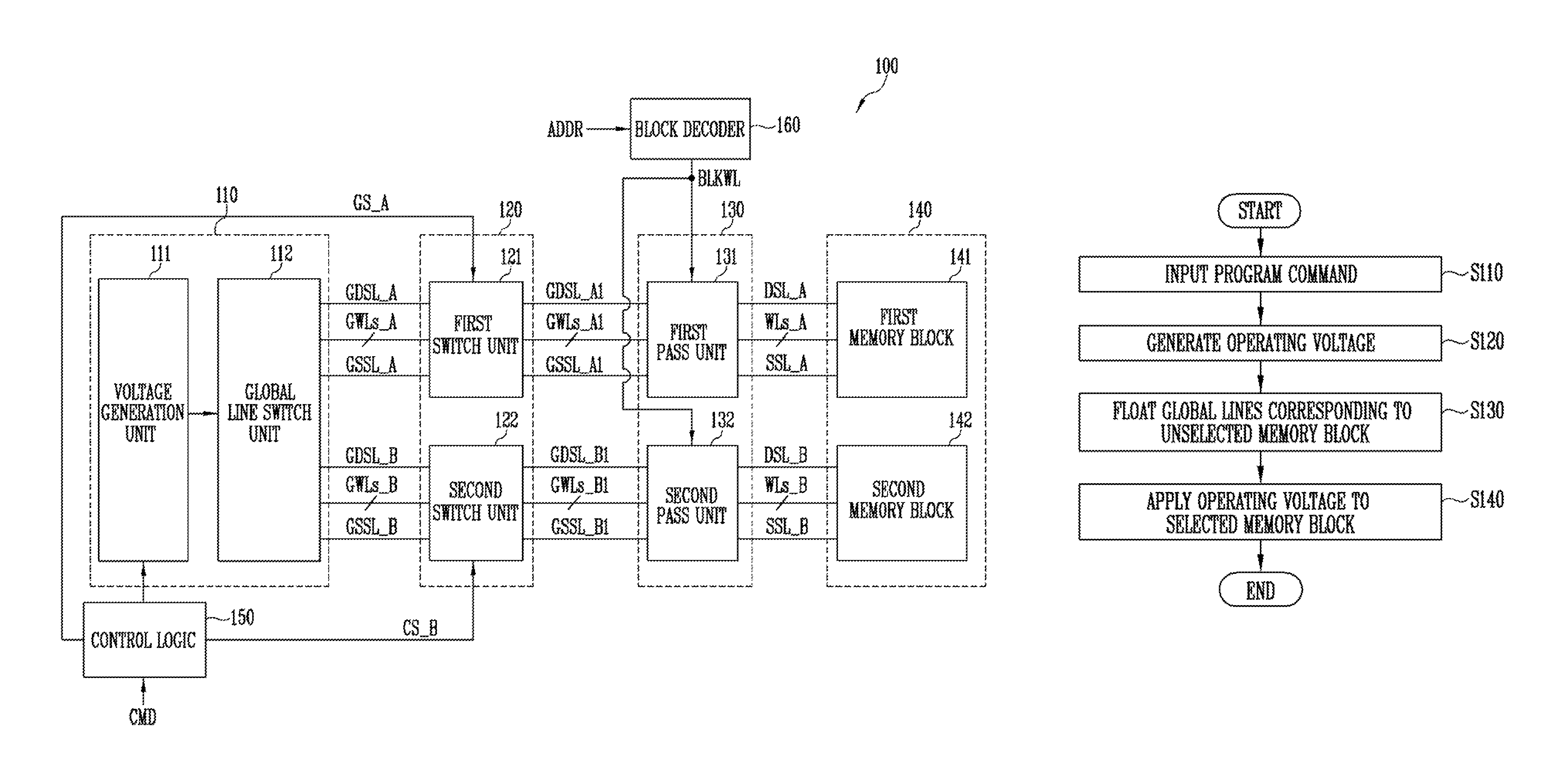
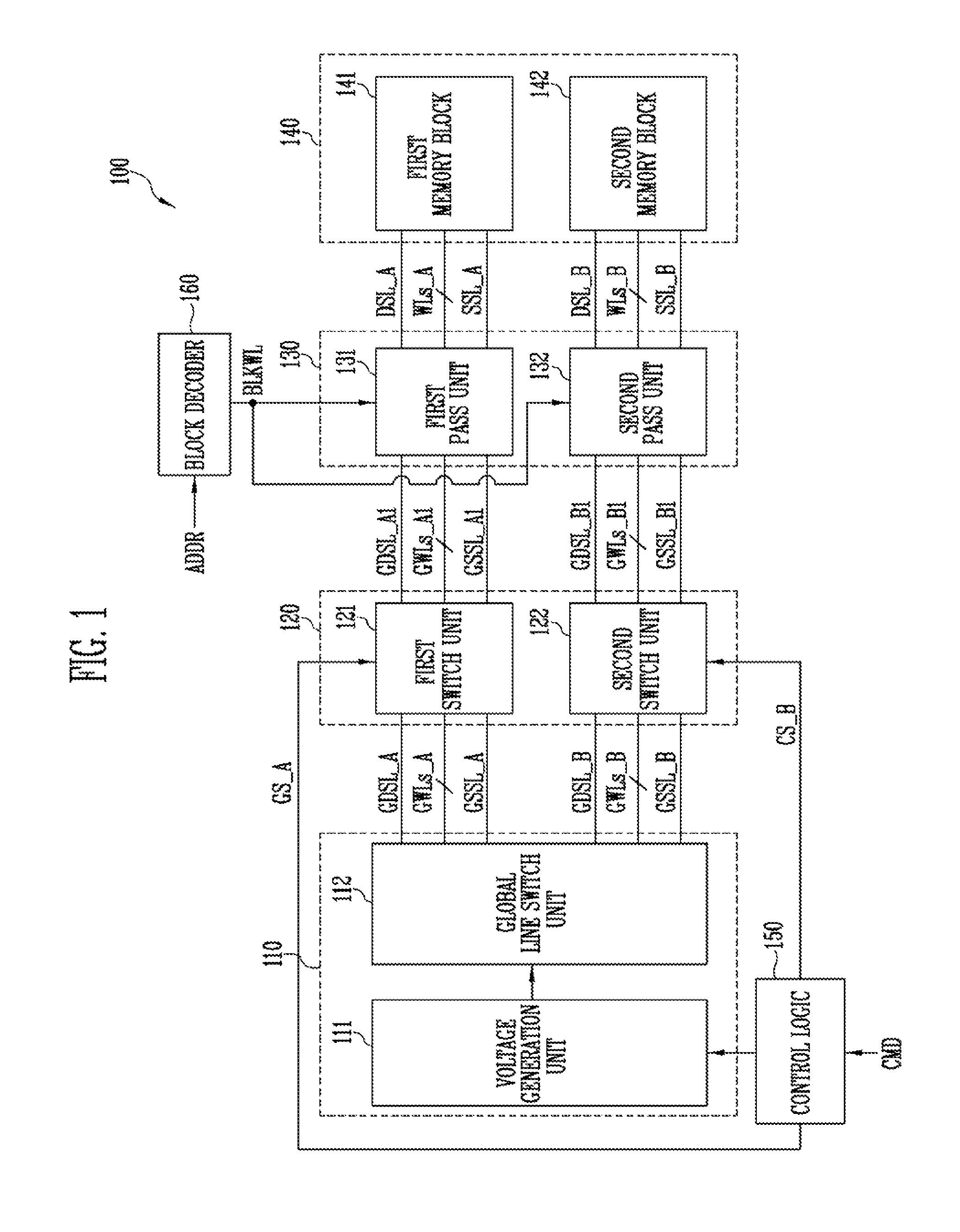
[0022]Hereinafter, various exemplary embodiments of the invention will be described in detail with reference to the accompanying drawings. In the drawings, thicknesses and lengths of components may be exaggerated for convenience of illustration. In the following description, a detailed explanation of related functions and constitutions may be omitted for simplicity and conciseness. Like reference numerals refer to like elements throughout the specification and drawings.

[0023]It is also noted that in this specification, “connected / coupled” refers to one component not only directly coupling another component but also indirectly coupling another component through an intermediate component.

[0024]Referring now to FIG. 1, a semiconductor memory device 100 is provided, according to an embodiment of the invention. The semiconductor memory device 100 may include a power supply unit 110, a switch circuit 120, a pass circuit 130, a memory unit 140, a control logic 150 and a block decoder 160.

[...


PUM


Abstract

A semiconductor memory device includes a memory unit including a first memory block and a second memory block, a power supply unit suitable for applying a plurality of operating voltages to one of first global lines or second global lines, a switching circuit suitable for switching the first global lines and first internal global lines in response to a first control signal and switching the second global lines and second internal global lines in response to a second control signal, and a pass circuit suitable for electrically connecting the first internal global lines to word lines and selection lines of the first memory block and electrically connecting the second internal global lines to word lines and selection lines of the second memory block in response to a block selection signal.

Description

CROSS-REFERENCE TO RELATED APPLICATION[0001]The present application claims priority under 35 U.S.C. §119(a) to Korean patent application number 10-2015-0136176, filed on Sep. 25, 2015, the entire disclosure of which is incorporated herein by reference in its entirety.BACKGROUND[0002]1. Field of Invention[0003]Various embodiments of the invention relate to a semiconductor memory device.[0004]2. Description of Related Art[0005]Semiconductor memory devices may be classified into volatile memory devices and non-volatile memory devices.[0006]Volatile memory devices such as Static Random Access memory (SRAM), Dynamic RAM (DRAM) and Synchronous DRAM (SDRAM) do not retain data stored therein when power supply to the device is turned off. Non-volatile memory devices operate at relatively lower write and read speeds than volatile memory devices, but they retain the stored data regardless of power on / off conditions. Therefore, non-volatile memory devices are used to store data which need to be...

Claims


Application Information

Patent Timeline
Patent Type & Authority Patents(United States)
IPC IPC(8): G11C11/34G11C16/22G11C16/30G11C16/08
CPCG11C16/12G11C16/08G11C16/30G11C16/10G11C8/12G11C16/0483
Inventor LEE, HEE YOUL
Owner SK HYNIX INC
Why Eureka
Try Eureka