Substrate components for packaging IC chips and electronic device packages of the same

a technology of substrate components and electronic devices, applied in the direction of printed circuit stress/warp reduction, printed circuit aspects, printed circuit non-printed electric components association, etc., can solve the problems of package warpage, high cost, and high coefficient of thermal expansion (cte) , to achieve the effect of easy and efficient production of electronic device packaging

Active Publication Date: 2016-10-25
HU DYI CHUNG
View PDF6 Cites 0 Cited by
  • Summary
  • Abstract
  • Description
  • Claims
  • Application Information

AI Technical Summary

Benefits of technology

[0006]In view of the problems existing in the prior art, the present invention provides glass based substrate components for packaging IC chips so that production of electronic device packaging can be performed easily and efficiently. Sequential layer build-up (SBU) layers are formed on the glass substrate to scale up the electrical connections while providing mechanical stability and rigidity.

Problems solved by technology

As the proportion of dielectric materials used for build-up layer on fine patterning package substrates increases, the issue of coefficient of thermal expansion (CTE) tends to rise and stiffness is likely to decrease due to a thinner core layer.
Accordingly, package warpage may increase, and chip cracks and other packaging defects are prone to occur.
Another issue is singulation.
While glass substrates are not machined as easily as polymer substrate, some may be damaged during singulation.

Method used


Image

  • Substrate components for packaging IC chips and electronic device packages of the same
  • Substrate components for packaging IC chips and electronic device packages of the same
  • Substrate components for packaging IC chips and electronic device packages of the same

Examples


Embodiment Construction

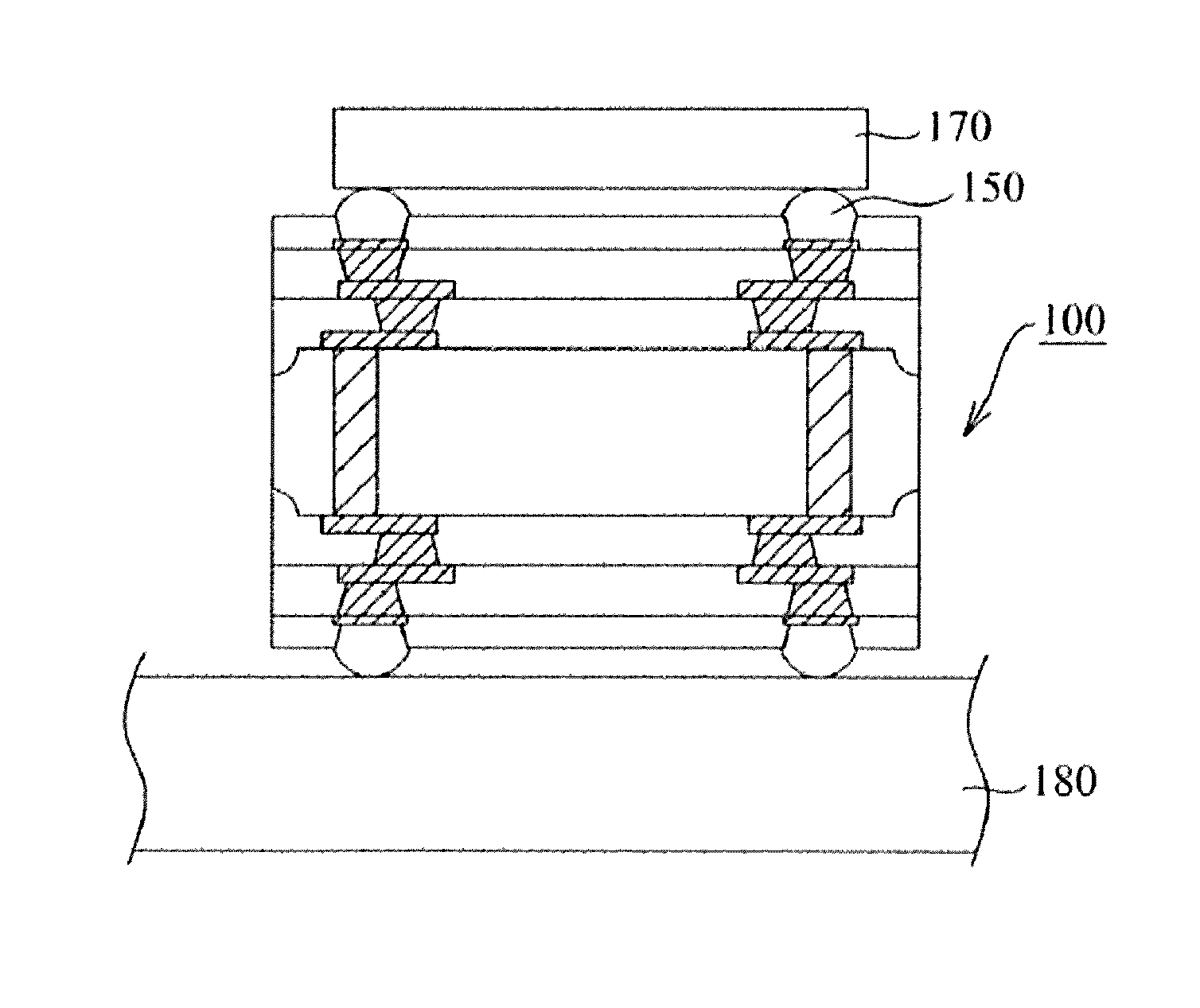
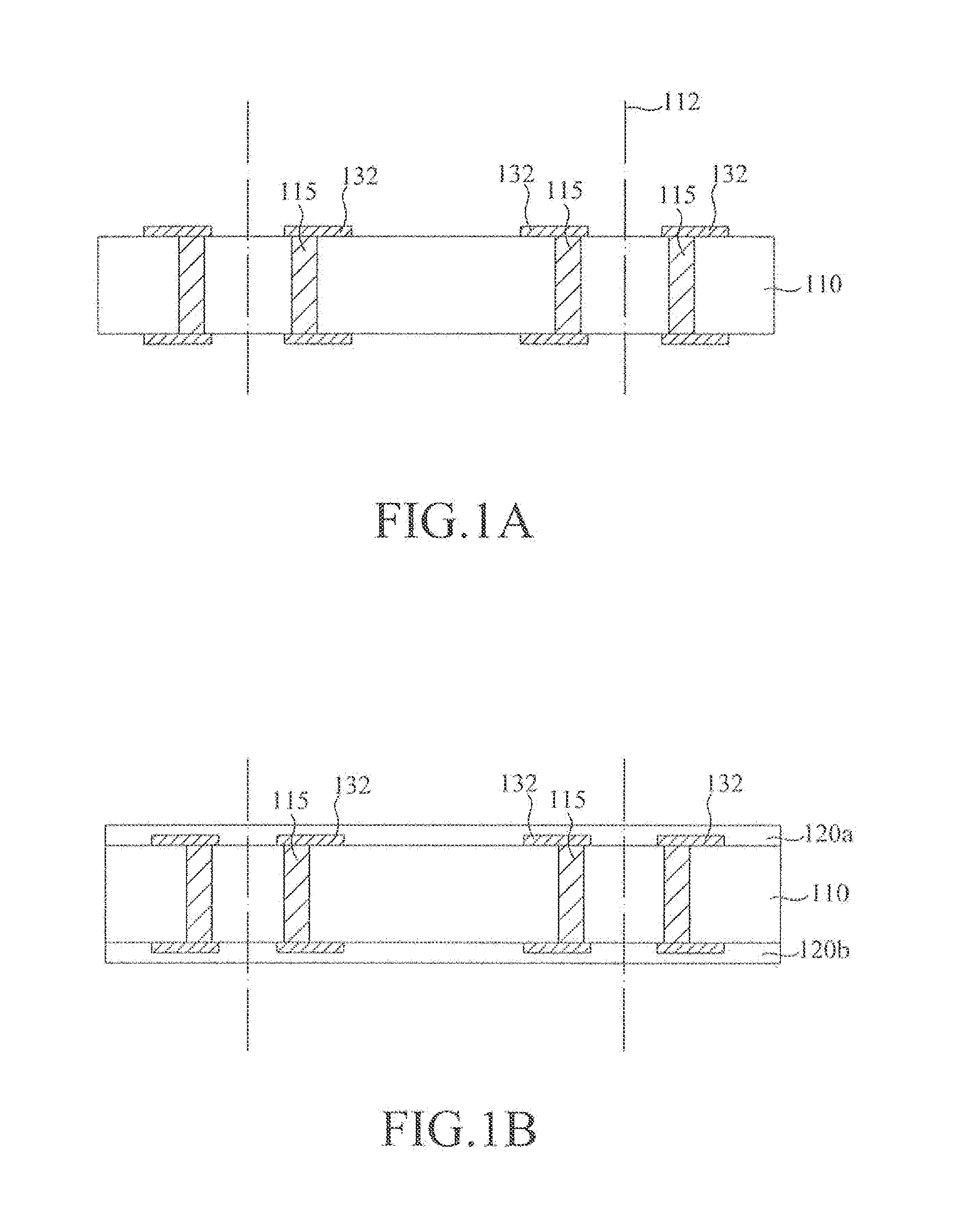
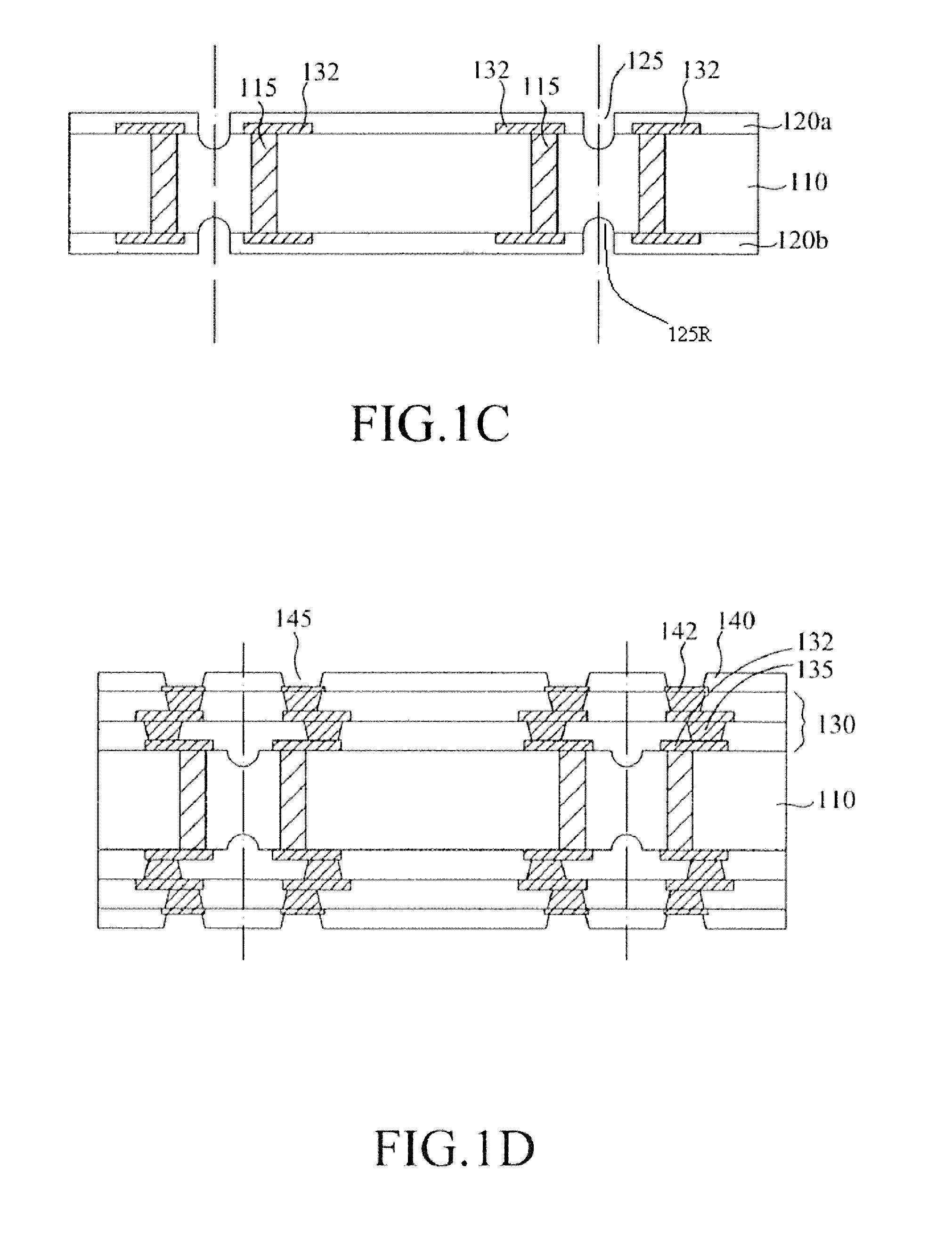
[0014]Reference will now be made in detail to the present preferred embodiments of the invention, examples of which are illustrated in the accompanying drawings. Wherever possible, the same reference numbers are used in the drawings and the description to refer to the same or like parts. In the drawings, the shape and thickness of an embodiment may be exaggerated for clarity and convenience. This description will be directed in particular to elements forming part of, or cooperating more directly with, apparatus in accordance with the present invention. It is to be understood that elements not specifically shown or described may take various forms well known to those skilled in the art. Further, when a layer is referred to as being on another layer or “on” a substrate, it may be directly on the other layer or on the substrate, or intervening layers may also be presented.

[0015]An embodiment of the present invention discloses a glass substrate component for packaging IC chips with refe...


PUM


Abstract

Substrate components for packaging IC chips and electronic device packages are disclosed. A substrate component for packaging IC chips comprises: a glass core base with at least one conductive through via connecting a combination of metallization and dielectric structures on both an upper surface and a lower surface of the glass core base; and, tapered edges created at a peripheral region of the glass core base; wherein dielectric layers are disposed over the tapered edges at the peripheral region of the glass core base. In accordance with an embodiment of the invention, the dielectric layers have a substantial planar upper surface, a lower surface conformably interfaced with the tapered edges at peripheral region of the glass core base, and a steep cutting face with the tapered edges of the glass core base. Alternatively, the tapered edges at peripheral region of the glass core base are not covered by the dielectric layers, and an encapsulated material sealing the tapered edges at peripheral region of the glass core base.

Description

FIELD OF INVENTION[0001]The present invention relates to electronic device packaging, and more particularly, to substrate components for packaging IC chips and electronic device packages containing the substrate component.BACKGROUND OF THE INVENTION[0002]Electronic device packages, particularly integrated circuit (IC) packages for consumer and industry applications are required to support the rapid growth of smart phones, tablets and other portable electronic devices. Electronic device packaging is arguably one of the most materials-intensive applications today. Package substrates also referred as chip carriers serve to protect the fragile IC chips and scale up the electrical connections while providing mechanical stability and rigidity. In some conventional applications, smaller and / or more reliably packaged devices can be fabricated, resulting in a larger number of units fabricated in parallel in the batch process.[0003]Requirements for coefficient of thermal expansion (CTE) match...

Claims


Application Information

Patent Timeline
Patent Type & Authority Patents(United States)
IPC IPC(8): H01L23/15H05K1/18H05K1/03H05K1/02H05K1/11H05K3/00H05K3/46
CPCH01L23/15H05K1/0271H05K1/0284H05K1/0306H05K1/111H05K1/112H05K1/181H05K3/0052H01L2224/16225H01L2924/15311H05K3/4605H05K2201/068H05K2201/0909H05K2201/09154H01L23/13H01L23/145H01L23/49816H01L23/49822H01L23/49827
Inventor HU, DYI-CHUNG
Owner HU DYI CHUNG
Why Eureka
Try Eureka