Gate drive circuit

a technology of drive circuit and liquid crystal display device, which is applied in the field of display, can solve the problems of shortened service life and adverse influence on circuit service life, and achieve the effect of improving the service life of the goa circui

Active Publication Date: 2016-11-01
TCL CHINA STAR OPTOELECTRONICS TECH CO LTD
View PDF13 Cites 6 Cited by
  • Summary
  • Abstract
  • Description
  • Claims
  • Application Information

AI Technical Summary

Benefits of technology

[0008]A technical problem to be solved by the present disclosure is to provide a unipolar low temperature poly-silicon (LTPS) based gate drive circuit, so that the service life of a GOA circuit can be improved.
[0040]As compared with an existing GOA drive unit, the present disclosure has the following advantages.
[0041]1. The pull-down holding part according to the present disclosure is configured as having a three phase voltage-dividing mode, so that suitable potentials of point P(N) and point K(N) during a working period and a non-working period of the circuit can be guaranteed. In this case, lower potential will be provided to P(N) and K(N) during a working period of a current stage of GOA unit, so that electric leakage from Q(N) and G(N) can be effectively prevented. In the meantime, a suitably high potential is provided to P(N) and K(N) during a non-working period, so that Q(N) and G(N) can be kept at a low potential during the non-working period.
[0042]2. According to the present disclosure, a gate line signal G(N) controls a transfer between a former stage and a latter stage, which does not require ST(N) cascade transmission signal of a conventional GOA drive circuit. As a result, the circuit configuration can be effectively simplified, the space for wiring can be saved, and the power consumption can be reduced.
[0043]3. According to the present disclosure, Darlington transistors are used in the control submodules of the pull-down holding part, so that electric leakage from P(N) and K(N) during the non-working period can be alleviated, and the pulling-down of the potentials of G(N) and Q(N) can be more smooth.
[0044]4. In the pull-down holding part according to the present disclosure, the control signal for controlling the two pull-down holding modules to work alternately is configured as low frequency pulse signal, so that the power consumption of the entire GOA drive circuit can be effectively reduced. Further, because the low frequency pulse signal, rather than a clock signal, is used to control the two pull-down holding modules to work alternately, a duty ratio of the clock signal can be flexibly configured according to different components and product models.

Problems solved by technology

However, the long working time of the pull-down holding part would have adverse influence on the service life of the circuit.
Furthermore, as for a large size LTPS display panel, due to large RC load of the GOA circuit, the service life thereof will also be shortened.

Method used


Image

  • Gate drive circuit
  • Gate drive circuit
  • Gate drive circuit

Examples


example 1

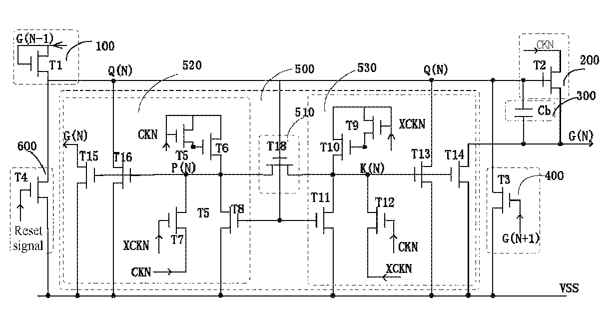
[0057]FIG. 1 schematically shows of a circuit configuration of a gate driver on array (GOA) drive unit according to example 1 of the present disclosure. FIG. 1 shows one of the multiple stages of GOA drive units indicated as N. For easy illustration, a stage before said GOA drive unit N is indicated as N−1, and a stage thereafter is indicated as N+1.

[0058]The GOA drive unit as shown in FIG. 1 comprises a pull-up control part 100, a pull-up part 200, a boost part 300, a key pull-down part 400, a pull-down holding part 500, and a circuit reset part 600.

[0059]The pull-up control part 100 comprises a pull-up control transistor T1. A gate of the pull-up control transistor T1 is short circuited with a first end thereof, and receives a gate signal G(N−1) outputted from a (N−1)th stage of GOA unit, and outputs a pull-up control signal G(N−1).

[0060]The pull-up part 200 comprises a pull-up transistor T2. A gate of the pull-up transistor T2 is coupled to an output end (point Q(N) in the drawin...

example 2

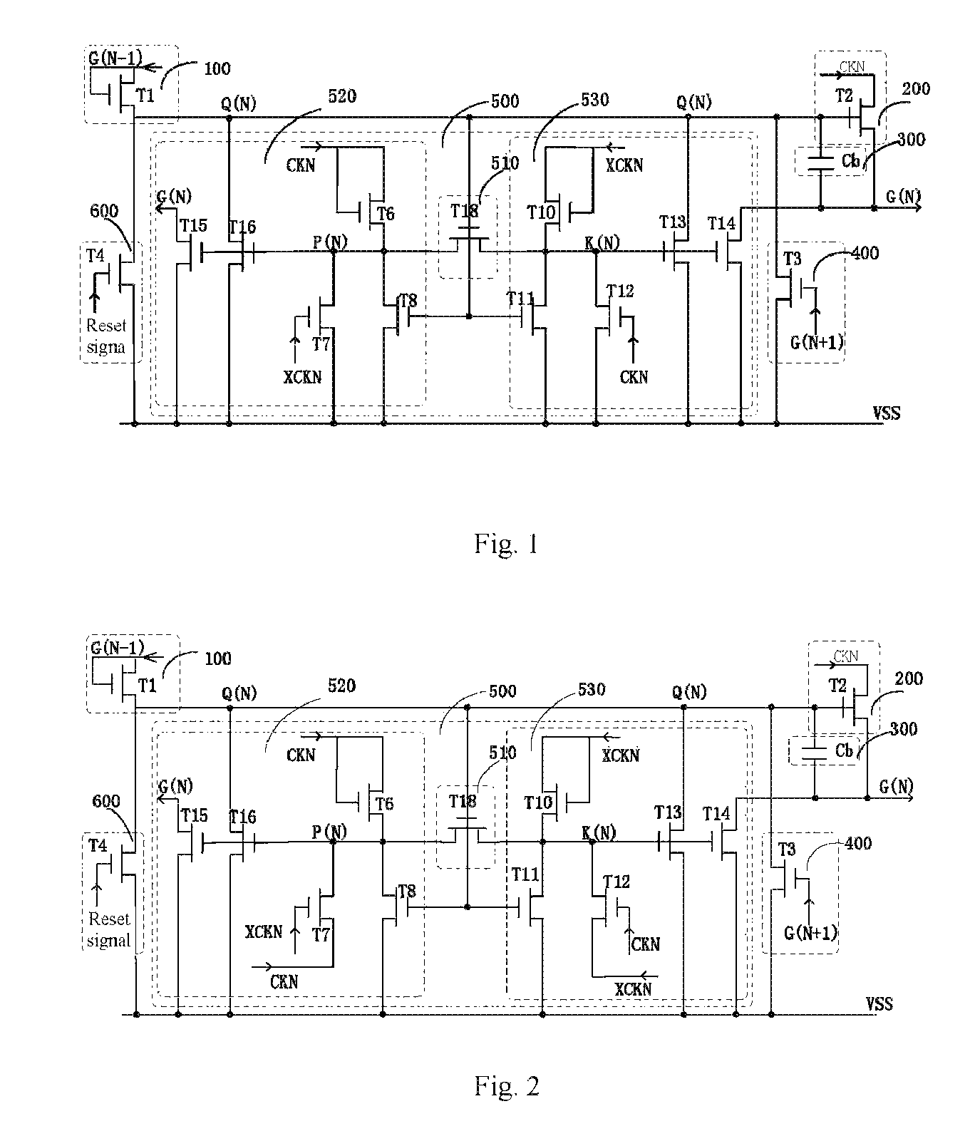
[0082]FIG. 2 schematically shows a circuit configuration of a gate driver on array drive unit according to example 2 of the present disclosure. The circuit is based on the circuit as shown in FIG. 1, with improvements on the pull-down holding part 500 thereof. Specifically, a source of a third transistor T7 receives a first control signal CKN, and a source of a fourth transistor T12 receives a second control signal XCKN. An absolute value of a low potential of CKN and that of XCKN are configured larger than an absolute value of a potential of a direct current power source VSS, thereby a force for pulling down the potential within a non-working period can be made stronger through the low potentials of CKN and XCKN.

example 3

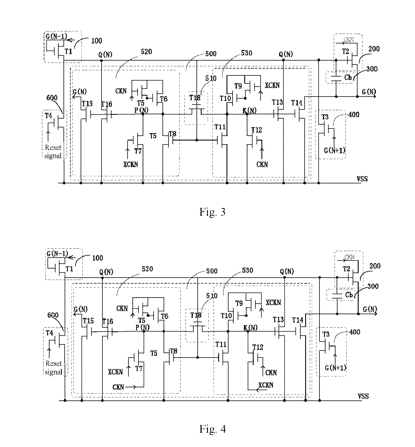
[0083]FIG. 3 schematically shows a circuit configuration of a gate driver on array drive unit according to example 3 of the present disclosure. The circuit is based on the circuit as shown in FIG. 1, with improvements on the pull-down holding part 500 thereof. Specifically, the circuit according to the present example further comprises transistors T5 and T9, so that T5 and T6 constitute a first Darlington transistor, and T9 and T10 constitute a second Darlington transistor.

[0084]A base of the first Darlington transistor is short circuited with a first end thereof for receiving a first control signal CKN, and a second end thereof is coupled to an output end P(N) of pull-down holding control signal of a first pull-down holding module. Specifically, a gate of transistor T5 is short circuited with a first end thereof for receiving the first control signal CKN. A gate of transistor T6 is coupled to a second end of transistor T5, a first end thereof is coupled to the gate of T5, and a sec...


PUM


Abstract

A gate drive circuit comprising multistage gate drive on array (GOA) drive units is provided. Each stage of GOA drive unit comprises a pull-up control part, a pull-up part, a key pull-down part, and a pull-down holding part. The pull-down holding part comprises a bridging module, a first and a second pull-down holding modules. When the bridging module is in a shutoff state, the first and the second pull-down holding modules work alternately, whereby a potential at the gate signal output end and / or a potential at the control end of the pull-up part are / is kept at a potential of the direct current power source according to a pull-down holding control signal.

Description

CROSS REFERENCE TO RELATED APPLICATION[0001]The present application claims benefit of Chinese patent application CN 201410804017.2, entitled “Gate Drive Circuit” and filed on Dec. 19, 2014, which is incorporated herein by reference on its entirety.TECHNICAL FIELD[0002]The present disclosure relates to the technical field of display, and in particular, to a gate drive circuit of a liquid crystal display device.TECHNICAL BACKGROUND[0003]In the prior art, a gate drive circuit is usually formed on an array substrate through gate driver on array (GOA) technology during manufacturing of an array of a liquid crystal display panel, thereby realizing progressive scan driving of gate lines. Based on this technology, a bonding procedure of an external IC can be omitted, and the integration level of the liquid crystal display panel can be improved.[0004]GOA circuit usually comprises multistage GOA units, each stage of GOA unit driving a corresponding horizontal scan line. Each stage of GOA unit...

Claims


Application Information

Patent Timeline
Patent Type & Authority Patents(United States)
IPC IPC(8): G09G3/36G11C19/28
CPCG09G3/3677G11C19/28G09G2300/0408G09G2310/0248G09G2300/0417G11C19/287
Inventor XIAO, JUNCHENG
Owner TCL CHINA STAR OPTOELECTRONICS TECH CO LTD
Why Eureka
Try Eureka