
Semiconductor circuit device, oscillator, electronic apparatus, and moving object

a technology of electromagnetic field and circuit device, applied in the direction of oscillator stabilization, oscillator generator, electrical apparatus, etc., can solve the problems of output frequency fluctuation, inaccurate detection of temperature of the vicinity of output buffer circuit, etc., and achieve the effect of reducing frequency fluctuation during activation and high reliability

Active Publication Date: 2016-11-01
SEIKO EPSON CORP
View PDF7 Cites 4 Cited by
  • Summary
  • Abstract
  • Description
  • Claims
  • Application Information

AI Technical Summary

Benefits of technology

This configuration reduces frequency fluctuations during activation, enabling high-frequency accuracy and reliability in oscillators, electronic apparatuses, and moving objects by ensuring efficient heat transfer and temperature detection.

Problems solved by technology

In JP-A-2007-67967, if the output buffer circuit which is one of heat generation sources is distant from the temperature sensor circuit, there is a possibility that a temperature of the vicinity of the output buffer circuit may not be accurately detected.
For this reason, for example, in a case where temperature compensation is performed on the basis of an output signal from the temperature sensor circuit when the TCXO is activated, correction based on a temperature of the output buffer circuit vicinity cannot be performed due to delay of transfer of heat to the temperature sensor circuit, and thus there is a possibility that an output frequency may fluctuate.

Method used


Image

  • Semiconductor circuit device, oscillator, electronic apparatus, and moving object
  • Semiconductor circuit device, oscillator, electronic apparatus, and moving object
  • Semiconductor circuit device, oscillator, electronic apparatus, and moving object

Examples


first specific example

1-2-1. First Specific Example

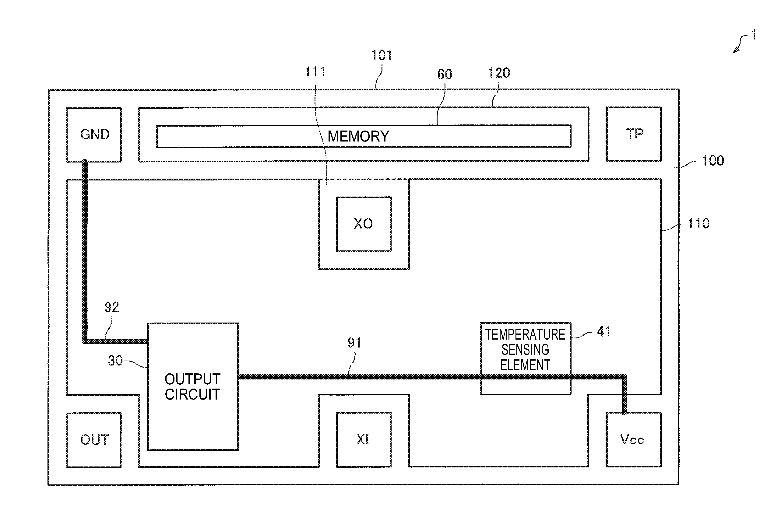
[0073]FIG. 8 is a plan view schematically illustrating a layout configuration of the semiconductor circuit device 1 related to a first specific example. In FIG. 8, some of the circuits included in the semiconductor circuit device 1 are not illustrated.

[0074]The semiconductor circuit device 1 related to the present specific example is configured to include a semiconductor substrate 100; a first circuit block 110 which includes at least the output circuit 30 and the temperature sensing element 41 disposed on the semiconductor substrate 100 as constituent elements; and a second circuit block 120 which includes at least the memory 60 disposed on the semiconductor substrate 100 as a constituent element. The semiconductor circuit device 1 is configured to include a first wiring 91 via which power for operating the output circuit 30 is supplied to the output circuit 30, and a second wiring 92 via which a reference voltage is supplied to the output circuit 30. T...

second specific example

1-2-2. Second Specific Example

[0090]FIG. 9 is a plan view schematically illustrating a layout configuration of the semiconductor circuit device 1 related to a second specific example. In FIG. 9, some of the circuits included in the semiconductor circuit device 1 are not illustrated. The same constituent elements as in the first specific example are given the same reference numerals, and detailed description thereof will be omitted.

[0091]As illustrated in FIG. 9, in the present specific example, the second wiring 92 overlaps the temperature sensing element 41 in a plan view.

[0092]According to the present specific example, heat generated from the output circuit 30 which is one of heat generation sources can be efficiently transferred to the temperature sensing element 41 via the second wiring 92. Therefore, even if the output circuit 30 is disposed to be spaced apart from the temperature sensing element 41, since the temperature sensing element 41 can efficiently detect heat generated...

third specific example

1-2-3. Third Specific Example

[0094]FIG. 10 is a plan view schematically illustrating a layout configuration of the semiconductor circuit device 1 related to a third specific example. In FIG. 10, some of the circuits included in the semiconductor circuit device 1 are not illustrated. The same constituent elements as in the first and second specific examples are given the same reference numerals, and detailed description thereof will be omitted.

[0095]As illustrated in FIG. 10, in the present specific example, the first wiring 91 and the second wiring 92 overlap the temperature sensing element 41 in a plan view.

[0096]According to the present specific example, heat generated from the output circuit 30 which is one of heat generation sources can be efficiently transferred to the temperature sensing element 41 via the first wiring 91 and the second wiring 92. Therefore, even if the output circuit 30 is disposed to be spaced apart from the temperature sensing element 41, since the temperat...


PUM


Abstract

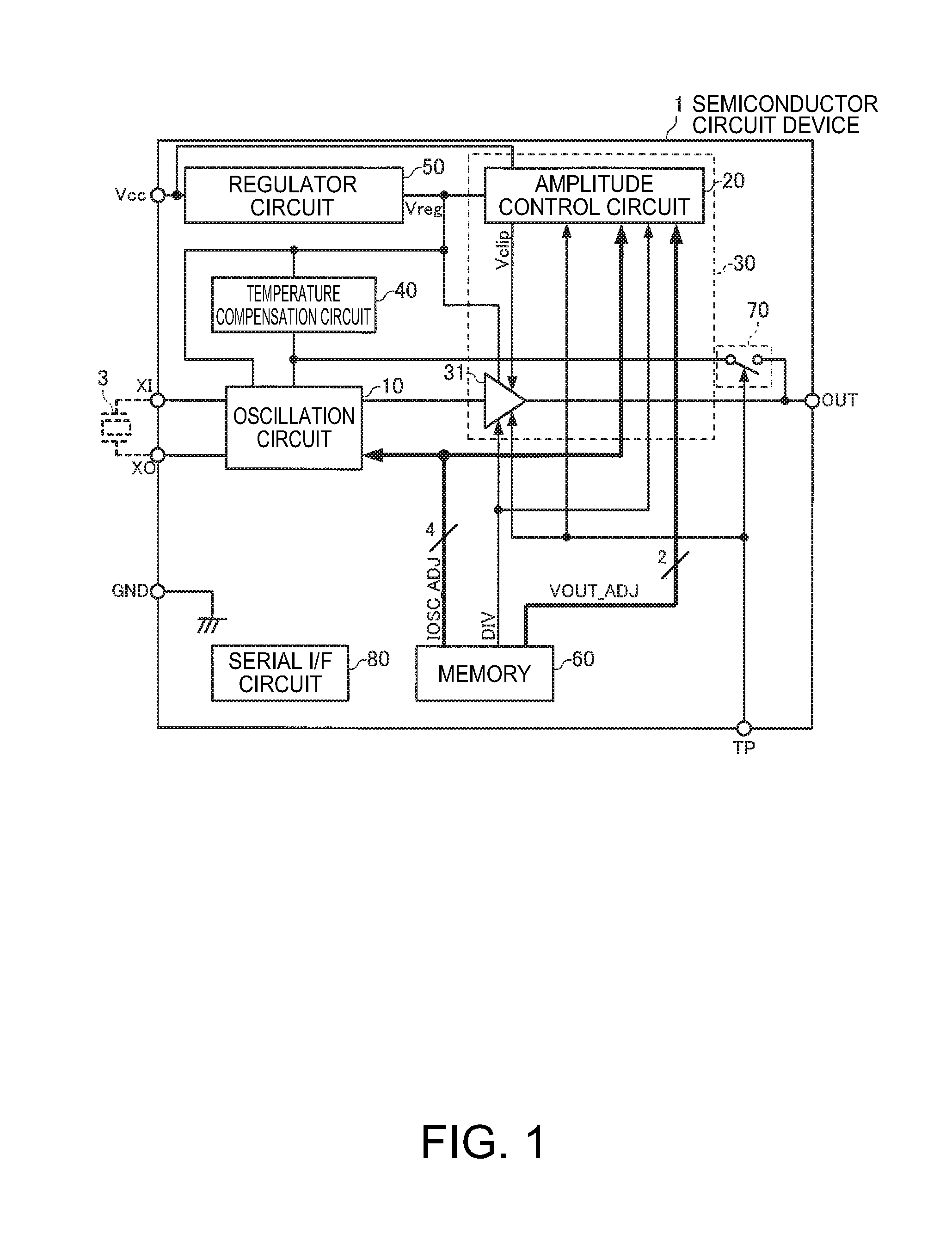
A semiconductor circuit device includes an oscillation circuit, an output circuit that outputs a signal output from the oscillation circuit, a temperature sensing element, a characteristic adjustment circuit that adjusts characteristics of the oscillation circuit on the basis of a signal output from the temperature sensing element, a first wiring via which power is supplied to the output circuit, and a second wiring via which a reference voltage is supplied to the output circuit in which at least one of the first wiring and the second wiring overlaps the temperature sensing element in a plan view.

Description

BACKGROUND[0001]1. Technical Field[0002]The present invention relates to a semiconductor circuit device, an oscillator, an electronic apparatus, and a moving object.[0003]2. Related Art[0004]In an AT cut quartz crystal resonator constituting a temperature compensated crystal oscillator (TCXO), a frequency fluctuates while drawing a curve approximated to a cubic curve which has an inflection point around 25° C. due to a change in ambient temperature. An oscillation circuit and the like constituting the oscillator also have temperature characteristics, and thus a frequency fluctuates due to influences thereof. In the TCXO, a voltage signal for compensating for the frequency fluctuation is generated by a temperature compensation circuit and is applied to a varicap diode provided in the oscillation circuit. Therefore, the frequency fluctuation due to the change in ambient temperature is minimized, and thus high frequency accuracy is realized.[0005]As an example of such a TCXO, JP-A-2007...

Claims


Application Information

Patent Timeline
Patent Type & Authority Patents(United States)
IPC IPC(8): H03B5/04H03B5/32H03L1/02
CPCH03L1/02H03B5/323H03B5/04H03B5/32H03B5/362H03B5/368H03B2200/0038H03L1/026
Inventor YAMAMOTO, TAKEHIRO
Owner SEIKO EPSON CORP
Learn More