
Light emitting diode module

a technology of light-emitting diodes and modules, which is applied in the direction of electroluminescent light sources, static indicating devices, instruments, etc., can solve the problems of voltage drop from the voltage source, erroneous grey level, and instability of the switching components used to control the operating current and the brightness of the light-emitting diodes

Active Publication Date: 2016-11-15
AU OPTRONICS CORP
View PDF11 Cites 0 Cited by
  • Summary
  • Abstract
  • Description
  • Claims
  • Application Information

AI Technical Summary

Benefits of technology

The pixel driving circuit of an OLED display in prior art is unstable because the switch components used to control the current flow and brightness of the light emitting diode are often biased after operating for a long time, resulting in erroneous grey levels. Additionally, as the size of the display increases, voltage drops from the voltage source deteriorate, which aggravates the instability of current flows and display quality. The technical effect of this patent is to provide a more stable and reliable pixel driving circuit for OLED displays.

Problems solved by technology

However, in a pixel driving circuit of an OLED display of prior art, switch components used to control an operating current and the brightness of a light emitting diode are a source of instability.
For example, the threshold voltage of a transistor is often biased after operating for along time, altering the current flowing through the light emitting diode and resulting in emitting an erroneous grey level.
Besides, as the size of the display increases, the voltage drop from the voltage source deteriorates.
This adds to the aging issue and worsens the instability of current flows and display quality.
Although there are some ways developed to compensate the threshold voltage bias, those methods lead to an increased number of switches and / or capacitors, lowering an aperture ratio of the display, and increasing the difficulty to design a driving circuit of a high resolution display.

Method used


Image

  • Light emitting diode module
  • Light emitting diode module
  • Light emitting diode module

Examples


first embodiment

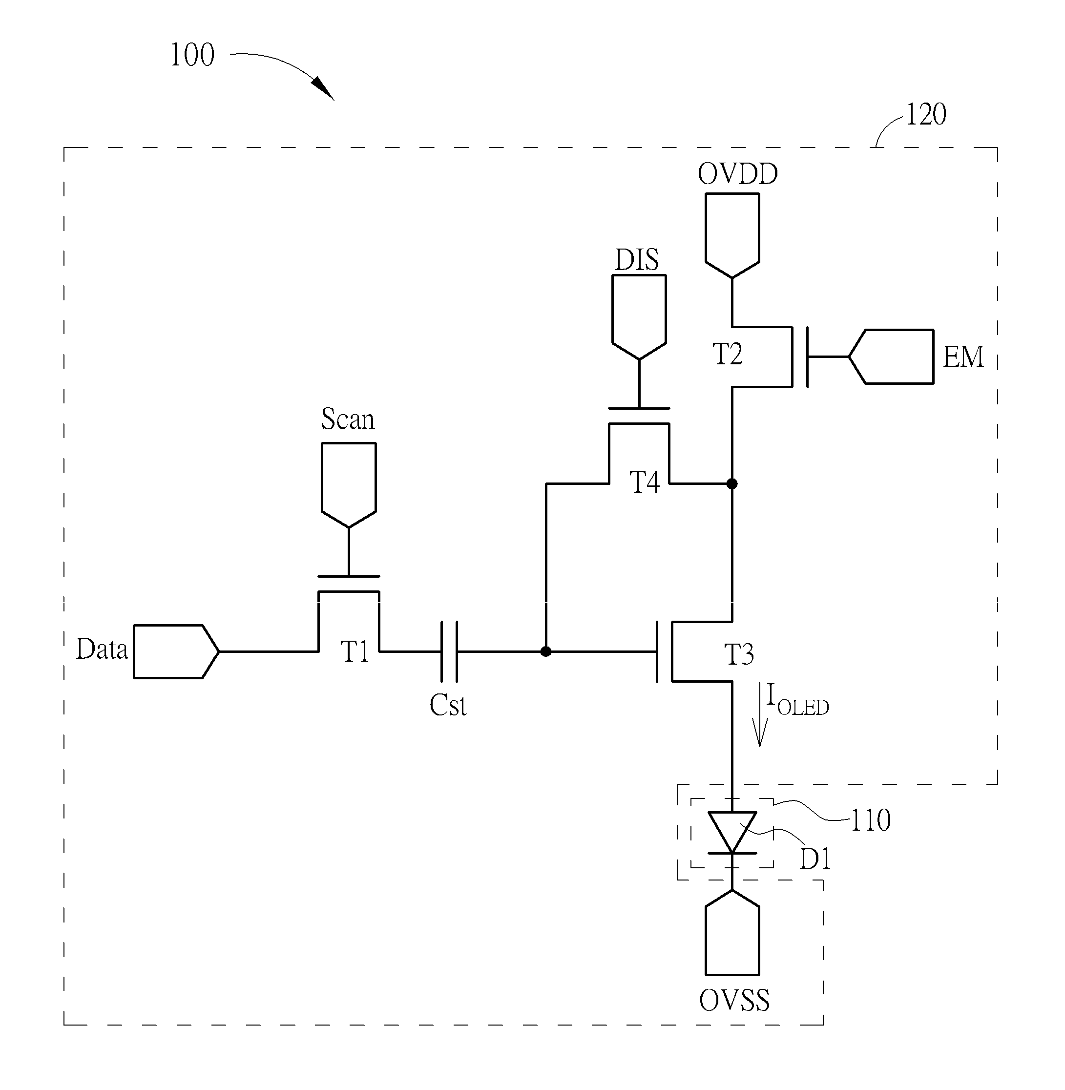
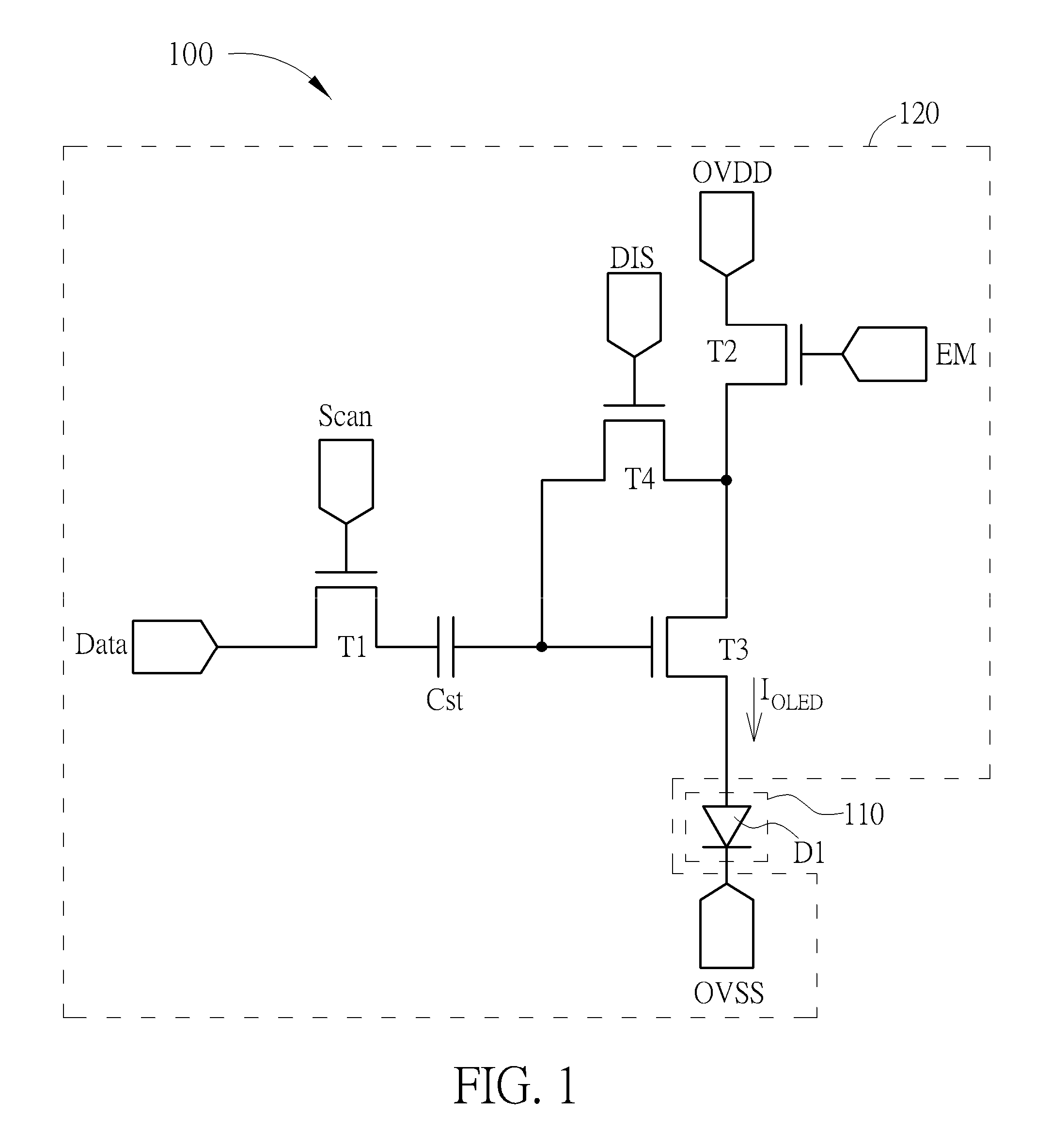
[0021]Please refer to FIG. 1 which shows a light emitting diode module 100 according to the present invention. As FIG. 1 shows, the light emitting diode module 100 comprises a light emitting unit 110 and a light emitting diode circuit 120. The light emitting unit 110 comprises a light emitting diode D1. The light emitting diode circuit 120 comprises a first transistor T1, a storage capacitor Cst, a second transistor T2, a third transistor T3, and a fourth transistor T4. The first transistor T1 has a first end configured to receive a data signal Data, a control end configured to receive a scan signal Scan, and a second end. The storage capacitor Cst has a first end coupled to the second end of the first transistor T1 and a second end. The second transistor T2 has a first end coupled to a first voltage source OVDD, a control end configured to receive an enable signal EM, and a second end. The third transistor T3 has a first end coupled to the second end of the second transistor T2, a ...

second embodiment

[0036]Please refer to FIG. 4 which shows the light emitting diode module 400 of the present invention. As shown in FIG. 4, the light emitting diode module 400 comprises a light emitting unit 410 and a light emitting circuit 420. The light emitting unit 410 comprises a light emitting diode D1. The difference between the light emitting diode modules 400 and 100 is the position of the light emitting diode D1. In the light emitting diode module 400, the light emitting diode D1 has a first end coupled to the first voltage source OVDD, and a second end. The second transistor T2 has a first end coupled to the second end of the light emitting diode D1, a control end configured to receive an enable signal EM, and a second end. The third transistor T3 has a first end coupled to the second end of the second transistor T2, a control end coupled to a second end of a storage capacitor Cst, and a second end coupled to a second voltage source OVSS.

[0037]Similarly, in the second embodiment, the curr...


PUM


Abstract

A light emitting diode module includes a light emitting unit and a light emitting diode circuit. The light emitting diode circuit includes four transistors and a storage capacitor. A first transistor includes a first end for receiving a data signal, and a control end. The storage capacitor has a first end coupled to a second end of the first transistor. A second transistor has a first end coupled to a first voltage source, and a control end. A third transistor has a first end coupled to a second end of the second transistor, and a control end coupled to a second end of the storage capacitor. A fourth transistor has a first end coupled to the second end of the storage capacitor, a control end, and a second end coupled to the second end of the second transistor.

Description

BACKGROUND OF THE INVENTION[0001]1. Field of the Invention[0002]The present invention relates to a light emitting diode module, and more particularly, a light emitting diode module which can generate a stable operating current.[0003]2. Description of the Prior Art[0004]Due to their slim shapes, low power consumption and low radiation, liquid crystal displays (LCDs) are widely applied in electronic devices such as notebooks, monitors, and PDAs (personal digital assistants). Besides, the organic light emitting diode (OLED) display can be operated without a backlight source and color filters, and has a slimmer shape and better performance in color, thus the OLED display is also widely used.[0005]However, in a pixel driving circuit of an OLED display of prior art, switch components used to control an operating current and the brightness of a light emitting diode are a source of instability. For example, the threshold voltage of a transistor is often biased after operating for along time...

Claims


Application Information

Patent Timeline
Patent Type & Authority Patents(United States)
IPC IPC(8): H05B33/08G09G3/32H05B44/00
CPCG09G3/3233H05B33/0806G09G2300/0814G09G2300/0819H05B45/30
Inventor HSU, WEI-CHULIU, LI-WEICHANG, HUA-GANG
Owner AU OPTRONICS CORP
Learn More