Photonic transceiving device package structure

a technology of transceivers and package structures, applied in the direction of optical elements, wavelength-division multiplex systems, instruments, etc., can solve the problems of serial link performance being limited by electrical bandwidth and electronic components of channels, continuously requiring a huge amount of bandwidth for transferring photo, video, music and other multimedia files, and achieving the effect of enhancing heat dissipation efficiency

Active Publication Date: 2016-11-15
MARVELL ASIA PTE LTD
View PDF4 Cites 31 Cited by
  • Summary
  • Abstract
  • Description
  • Claims
  • Application Information

AI Technical Summary

Benefits of technology

The present invention provides a photonic transceiver with a detachable package structure that allows for easy replacement of individual components. The PCB board and cylindrical element of the transmitting device can also be detached and detected individually for recycling and reuse. The reversed output orientation of the transmitting device makes it easy to couple with a silicon photonics chip on the PCB. The upside-down disposition of the transmitting laser device on PCB with its TEC base attached to the lid member away from the PCB enhances heat dissipation efficiency for the transmitting laser device.

Problems solved by technology

The patent text is about a new structure for a photonic transceiver package that solves the problem of limited bandwidth and transmission speed in traditional cable communication. The optical fiber transmission system replaces traditional communication transmission systems and has advantages of high speed transmission and long transmission distance. The text also discusses wavelength-division multiplexing (WDM) technology that doubles the transmission capacity of optical fibers by processing multiple optical carrier signals. However, the current light transmitter structure cannot be repaired for individual frequency, causing larger consumption in cost. The technical problem is to provide a more cost-effective and efficient solution for repairing individual frequency in the light transmitter structure.

Method used


Image

  • Photonic transceiving device package structure
  • Photonic transceiving device package structure
  • Photonic transceiving device package structure

Examples


Embodiment Construction

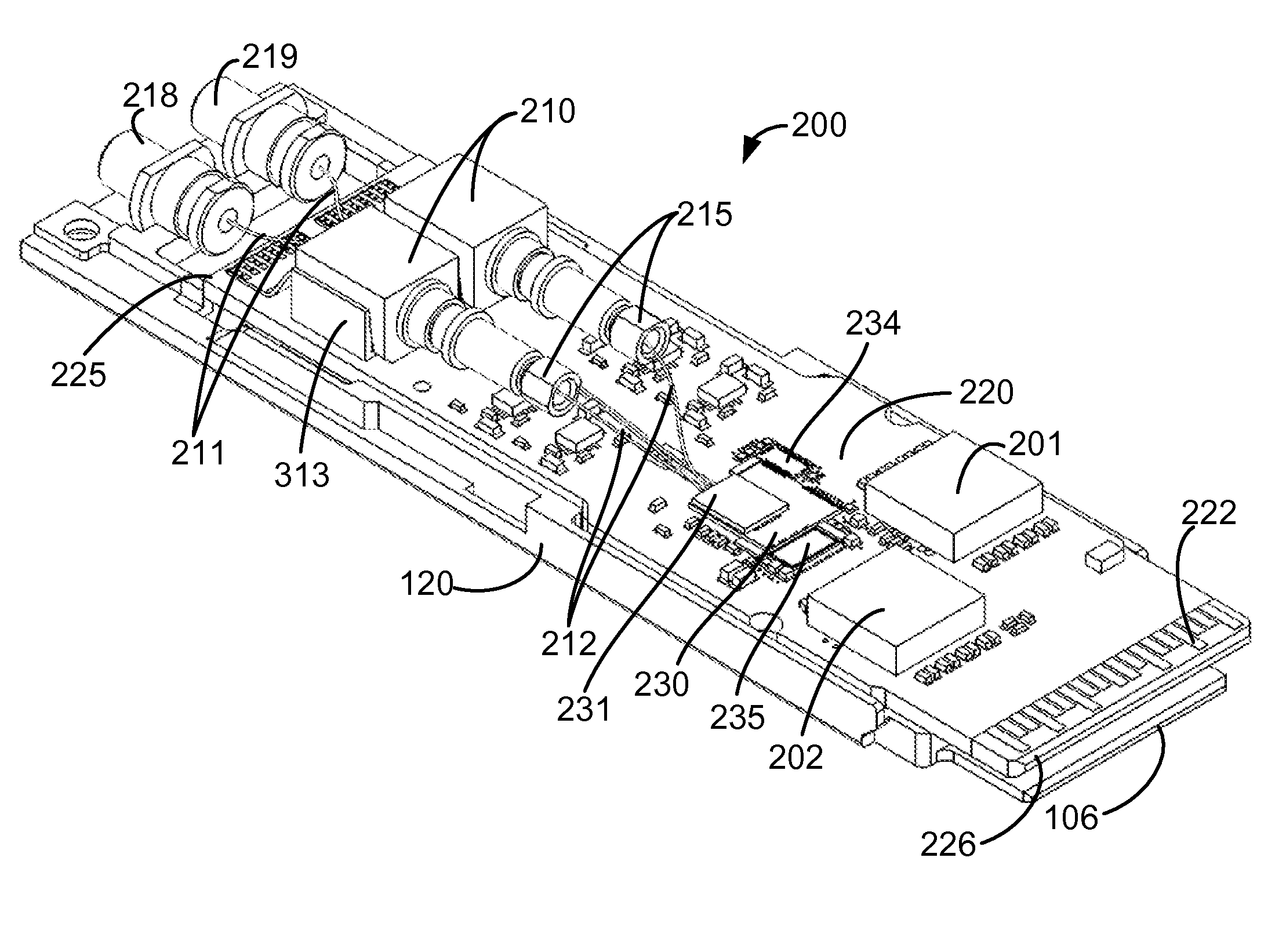
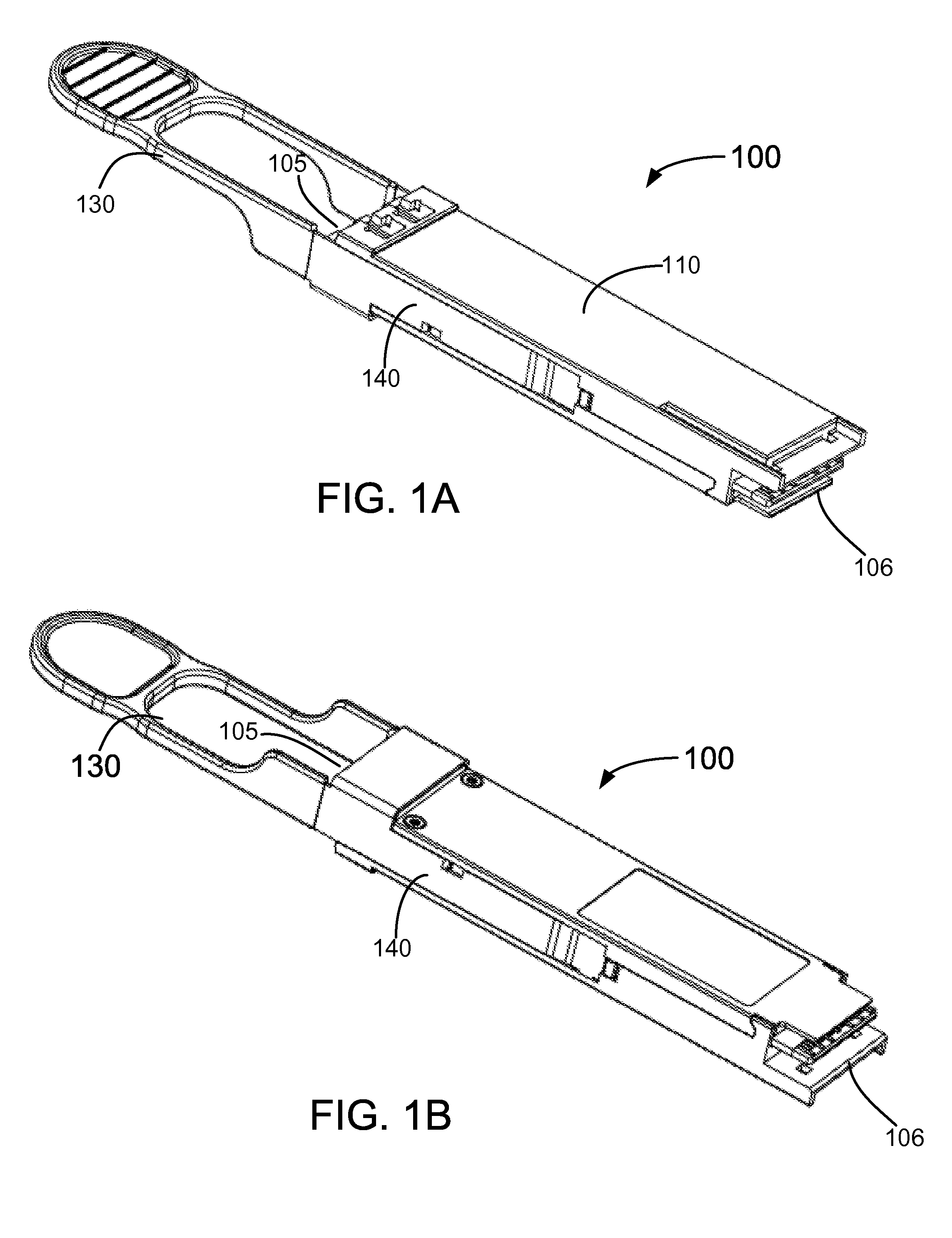
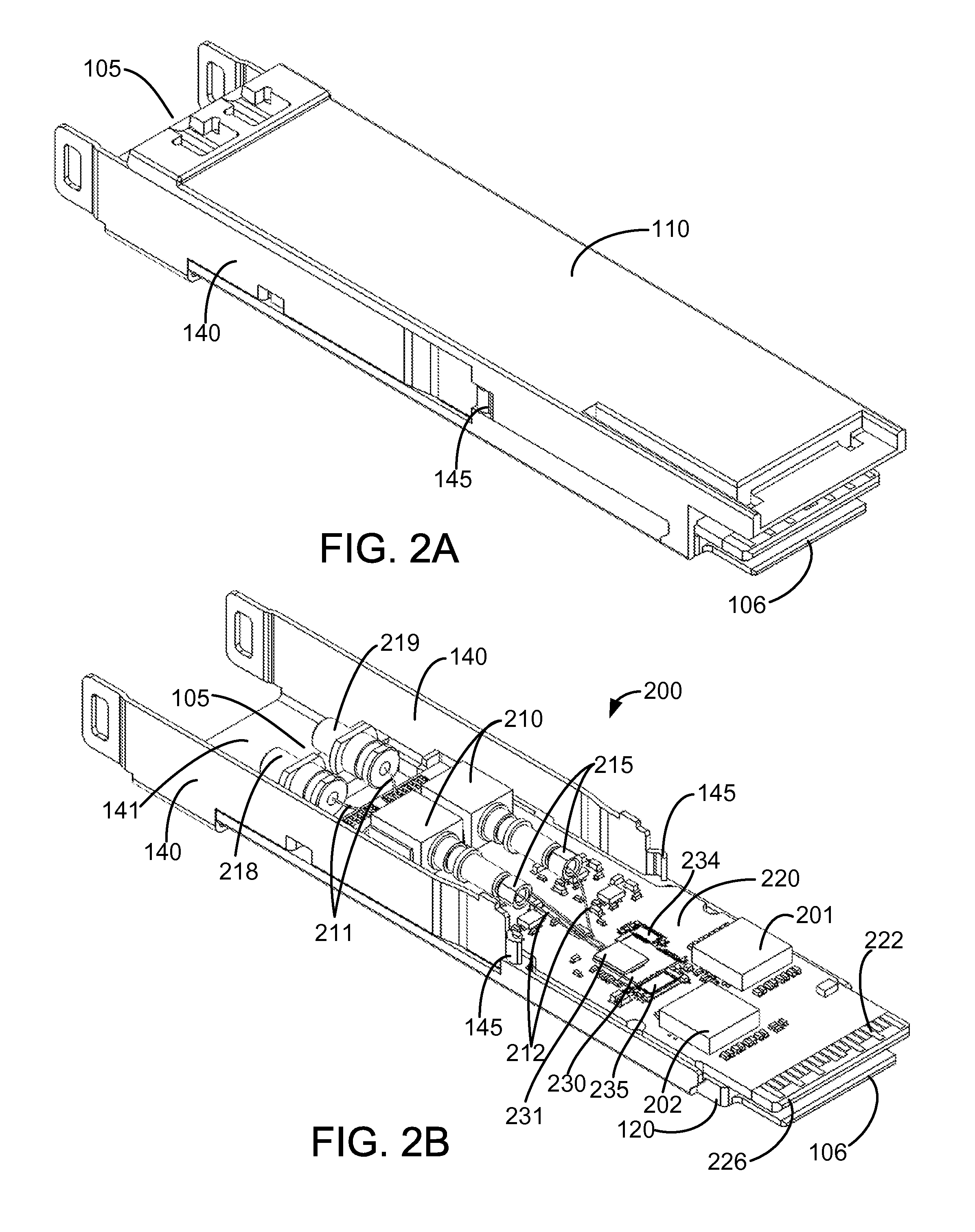
[0025]The present disclosure is related to a photonic transceiver package structure, more particularly, to a silicon photonic transceiver package structure in QSFP specification adapted with multiple TEC-TOSA laser devices disposed upside down to keep heat sinks away from PCB and laid reversely in orientation of laser output port relative to optical input / output port of the transceiver. In certain embodiments, the invention is applied for high bandwidth optical communication, though other applications are possible.

[0026]The following description is presented to enable one of ordinary skill in the art to make and use the invention and to incorporate it in the context of particular applications. Various modifications, as well as a variety of uses in different applications will be readily apparent to those skilled in the art, and the general principles defined herein may be applied to a wide range of embodiments. Thus, the present invention is not intended to be limited to the embodime...


PUM


Abstract

The apparatus includes a case having a base member, two partial side members, and a lid member to provide a spatial volume with an opening at a back end of the base member. Additionally, the apparatus includes a PCB installed inside the spatial volume over the base member with a pluggable connector at the back end. The apparatus includes one or more optical transmitting devices in transmit-optical-sub-assembly package, each being mounted upside-down on the PCB and including a built-in TEC module in contact with the lid member and a laser output port aiming toward the back end. Furthermore, the apparatus includes a silicon photonics chip including a fiber-to-silicon attachment module, mounted on the PCB and coupled to a modulation driver module and a trans-impedance-amplifier module. Moreover, the apparatus includes an optical input port and output port being back connected to the fiber-to-silicon attachment module.

Description


Claims


Application Information

Patent Timeline
Owner MARVELL ASIA PTE LTD
Why Eureka
Try Eureka