
Organic light-emitting device and lighting device with organic resin and glass substrate

a light-emitting device and organic resin technology, which is applied in the direction of organic semiconductor devices, solid-state devices, semiconductor lamp usage, etc., can solve the problems of lowering reliability, adversely affecting the lifetime of organic el elements and light-emitting devices in some cases, and achieve high reliability

Active Publication Date: 2016-11-22
SEMICON ENERGY LAB CO LTD
View PDF82 Cites 3 Cited by
  • Summary
  • Abstract
  • Description
  • Claims
  • Application Information

AI Technical Summary

Benefits of technology

The patent text aims to provide a light-emitting device that uses a plastic substrate and is highly reliable, despite the fact that plastic allows moisture, oxygen, and impurities to easily enter the device. The invention provides a solution to prevent this from happening and ensures the device has a long lifetime.

Problems solved by technology

An organic EL element has a problem in that the reliability is lowered owing to entry of moisture, oxygen, an impurity, or the like.
Therefore, entry of moisture, oxygen, an impurity, or the like from the side where the plastic substrate is used adversely affects the lifetime of the organic EL element and the light-emitting device in some cases.

Method used


Image

  • Organic light-emitting device and lighting device with organic resin and glass substrate
  • Organic light-emitting device and lighting device with organic resin and glass substrate
  • Organic light-emitting device and lighting device with organic resin and glass substrate

Examples


embodiment 1

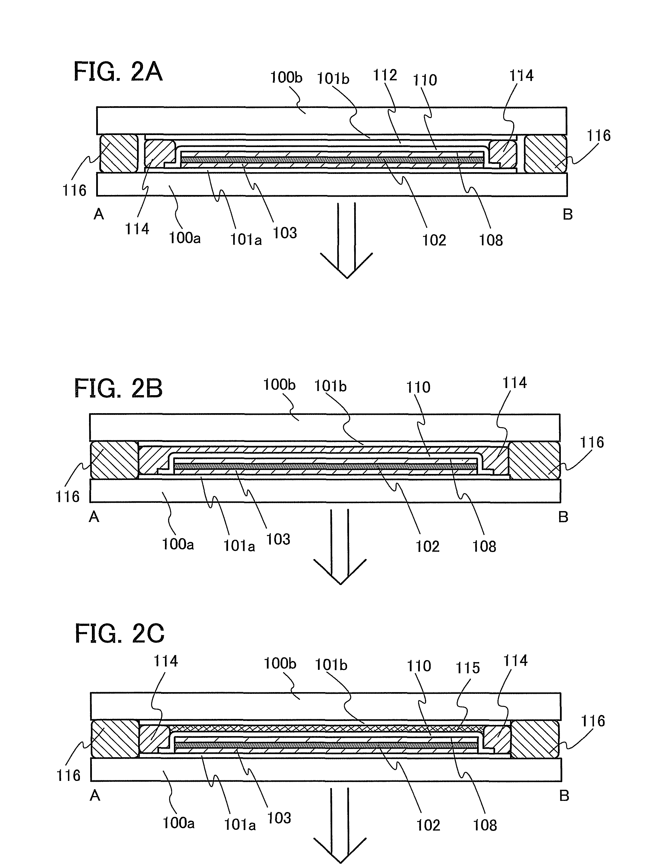
[0063]In this embodiment, a light-emitting device according to one embodiment of the present invention will be described with reference to FIG. 1, FIGS. 2A to 2C, FIG. 3, FIG. 4, and FIGS. 5A and 5B.

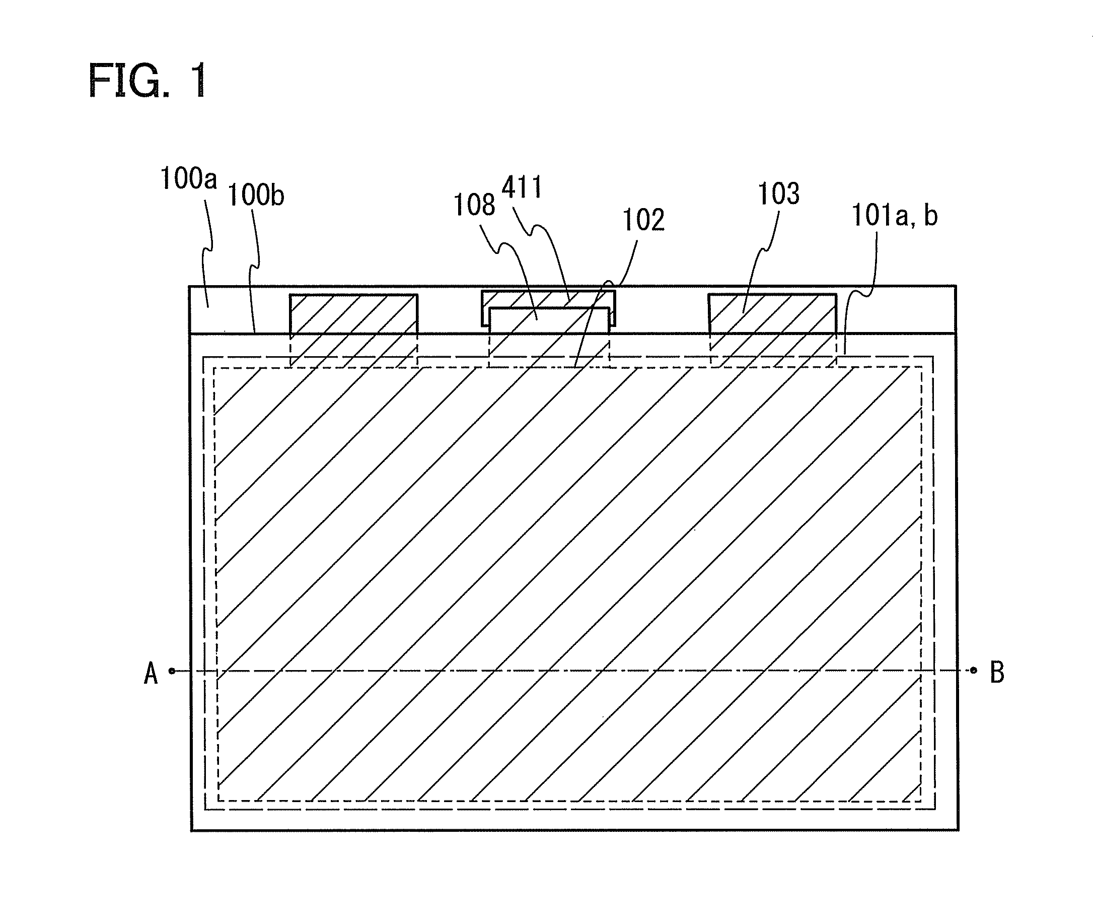
[0064]FIG. 1 is a plan view of a light-emitting device according to one embodiment of the present invention. Note that in FIG. 1, some components (e.g., a sealant 114 in FIG. 2A and the like) are not illustrated.

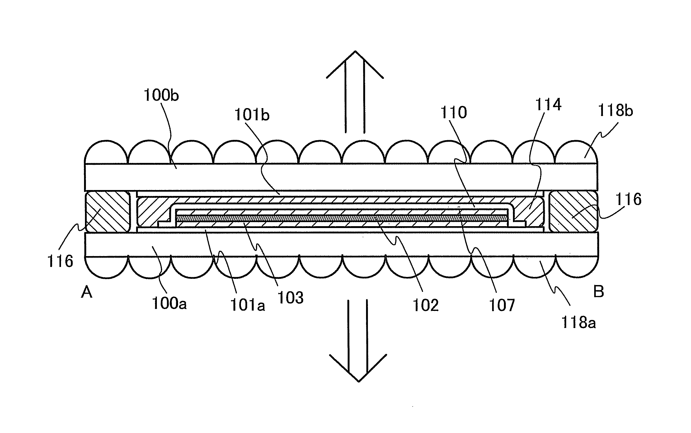
[0065]In FIG. 1, a first glass layer 101a is formed over a first organic resin layer 100a, and a light-emitting element (a first electrode 103, an EL layer 102, and a second electrode 108) is formed over the first glass layer 101a. In addition, a second glass layer 101b is formed over the light-emitting element, and a second organic resin layer 100b is formed over the second glass layer 101b.

[0066]The second electrode 108 is connected to a connection electrode 411. The connection electrode 411 can be formed using a material similar to that of the first electrode 103.

[0067]Furthe...

embodiment 2

[0114]In this embodiment, a manufacturing method of a light-emitting device according to one embodiment of the present invention which is described Embodiment 1 will be described with reference to FIGS. 7A to 7E and FIGS. 8A to 8D.

Manufacturing Method 1

Structural Example 1

[0115]One example of a manufacturing method of Structural Example 1 (see FIG. 2A) will be described with reference to FIGS. 7A to 7E.

[0116]First, the first glass layer 101a is formed over the first organic resin layer 100a with the use of an adhesive (FIG. 7A).

[0117]Next, the light-emitting element (the first electrode 103, the EL layer 102, and the second electrode 108) is formed over the first glass layer 101a.

[0118]The first electrode 103 and the second electrode 108 each can be formed by a sputtering method, an evaporation method (including a vacuum evaporation method), or the like. The EL layer 102 can be formed by an evaporation method (including a vacuum evaporation method), an inkjet method, a coating meth...

example 3

Structural Example 3

[0137]In the above manufacturing process of Structural Example 1, the second electrode is formed using a light-transmitting material. In such a manner, Structural Example 3 (see FIG. 4) can be manufactured. The other layers can be formed by forming methods similar to those in Structural Example 1.


PUM


Abstract

A highly reliable light-emitting device which includes an organic EL element and is lightweight is provided. The light-emitting device includes a first organic resin layer; a first glass layer over the first organic resin layer; a light-emitting element over the first glass layer; a second glass layer over the light-emitting element; and a second organic resin layer over the second glass layer. The first organic resin layer and the first glass layer each have a property of transmitting visible light. The light-emitting element includes a first electrode having a property of transmitting visible light, a layer containing a light-emitting organic compound, and a second electrode stacked in this order from the first glass layer side.

Description

BACKGROUND OF THE INVENTION[0001]1. Field of the Invention[0002]The present invention relates to a light-emitting device utilizing organic electroluminescence (EL). The present invention also relates to a lighting device including the light-emitting device.[0003]2. Description of the Related Art[0004]Research and development have been extensively conducted on an element utilizing an organic electroluminescence phenomenon (also referred to as an organic EL element). In the fundamental structure of the organic EL element, a layer containing a light-emitting organic compound is sandwiched between a pair of electrodes. By applying voltage to this element, light emission from the light-emitting organic compound can be obtained.[0005]The organic EL element can be formed into a film form and thus a large-area element can easily be formed. Therefore, utility value of the organic EL element as a surface light source that can be applied to lighting or the like is also high.[0006]For example, ...

Claims


Application Information

Patent Timeline
Patent Type & Authority Patents(United States)
IPC IPC(8): H01L51/52H01L51/50
CPCH01L51/5275H01L51/50H01L51/524H01L51/525H01L51/5212H01L51/5237H01L51/5246H01L51/5253H01L51/5256H01L51/5259H01L2251/50H01L2251/53H01L2251/5307H01L2251/5323H01L2251/5338H01L2251/5361H10K2102/3031H10K2102/311H10K59/874H10K59/8722H10K59/873H10K59/879H10K59/871H10K59/80516Y02B20/30H10K50/8426H10K50/00H10K50/84H10K50/814H10K50/841H10K50/844H10K50/846H10K50/858H10K50/8428H10K50/8445H10K2102/301H10K2102/302H10K2102/3023
Inventor YAMAZAKI, SHUNPEITANAKA, KOICHIROHIROKI, MASAAKIIKEDA, HISAOAKIMOTO, KENGO
Owner SEMICON ENERGY LAB CO LTD
Learn More