

Package structure
a packaging and structure technology, applied in the direction of printed circuit, conductive pattern formation, printed element electric connection formation, etc., can solve the problems of difficult formation of patterned circuit layers, high cost of sputtering, complex manufacturing methods, etc., to reduce the height-width ratio, enhance bonding strength, and simplify the manufacturing process of the package structure
- Summary
- Abstract
- Description
- Claims
- Application Information
AI Technical Summary
Benefits of technology
Problems solved by technology
Method used
Image

Examples
Embodiment Construction
[0030]Reference will now be made in detail to the present preferred embodiments of the invention, examples of which are illustrated in the accompanying drawings. Wherever possible, the same reference numbers are used in the drawings and the description to refer to the same or like parts.
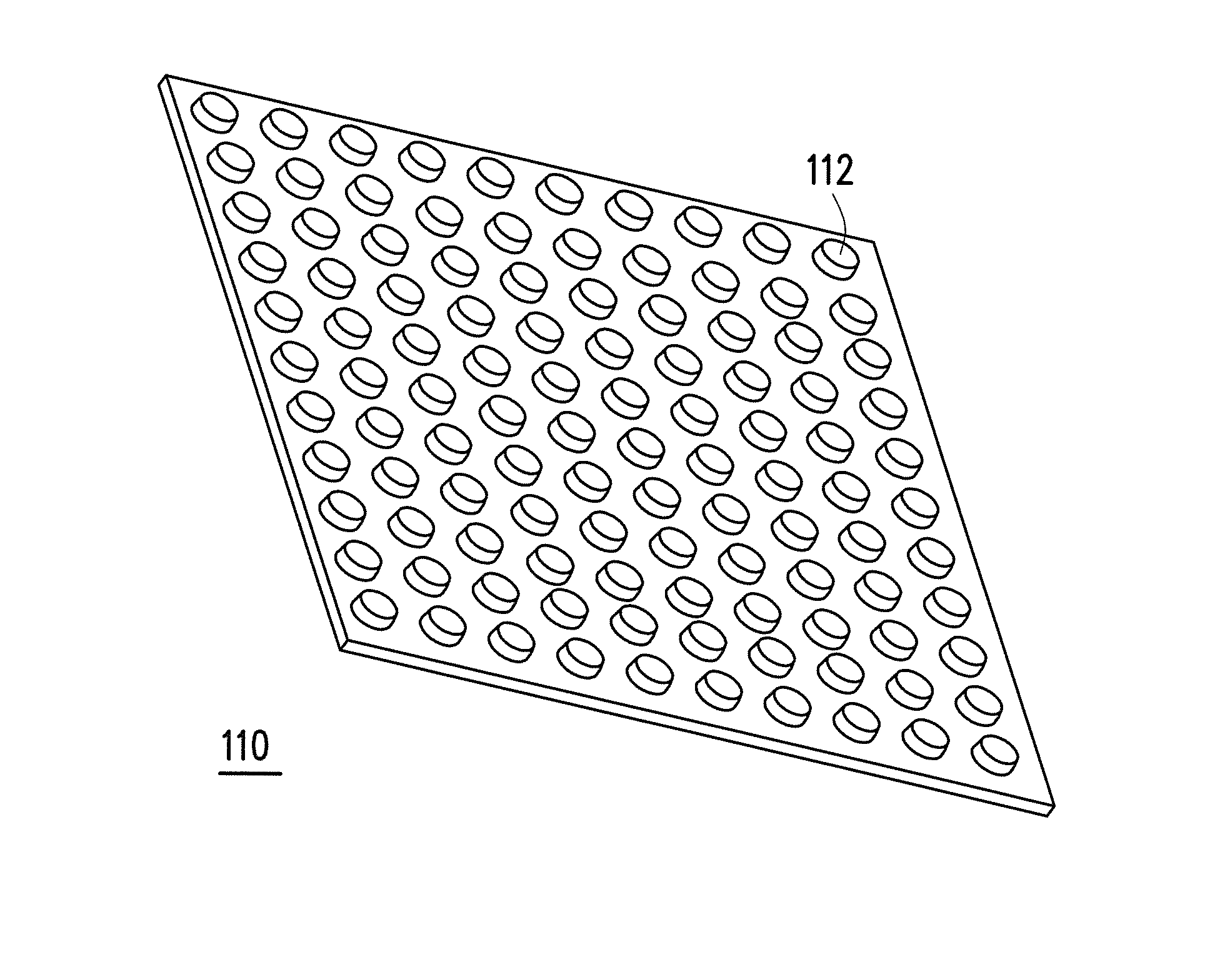
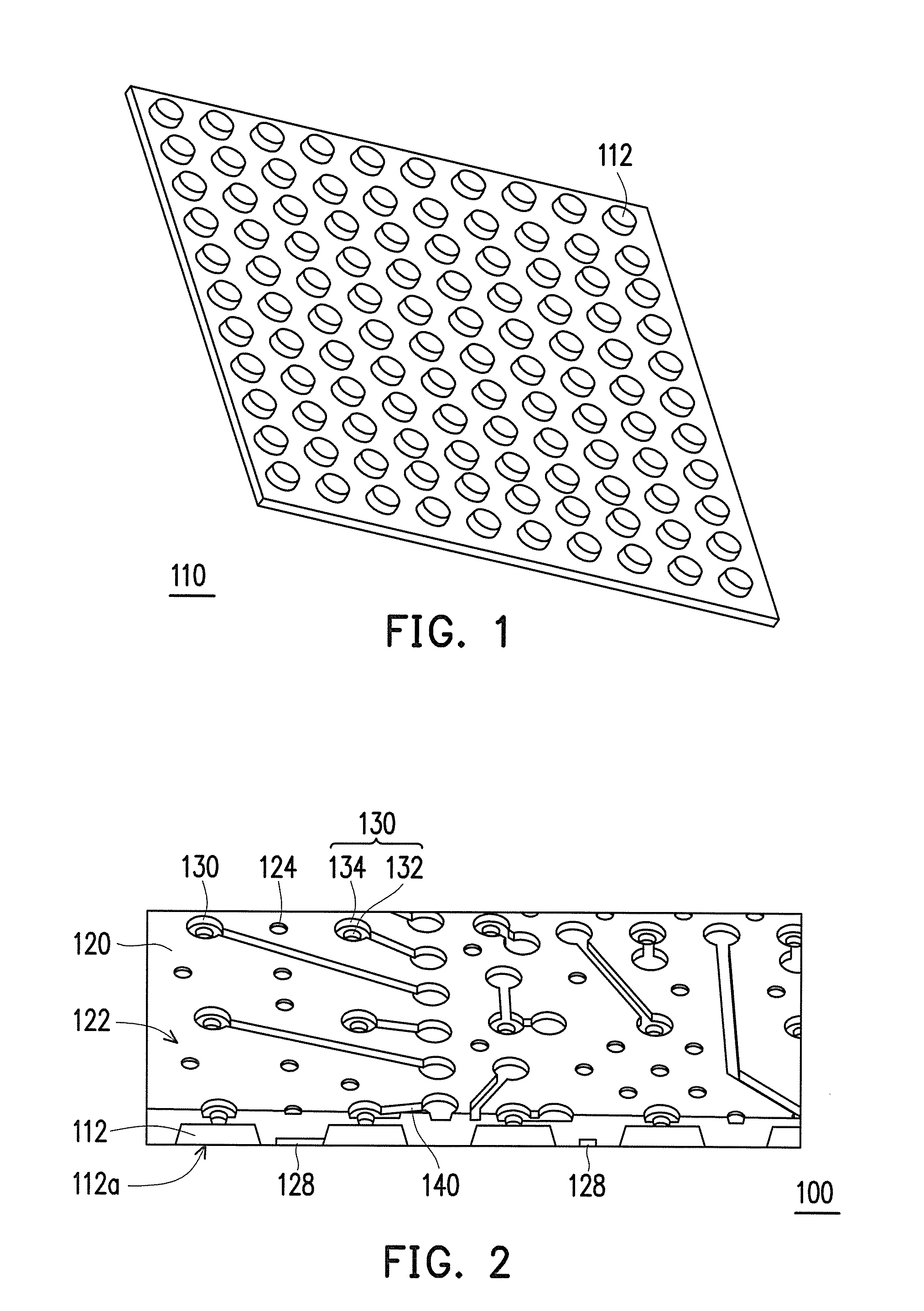
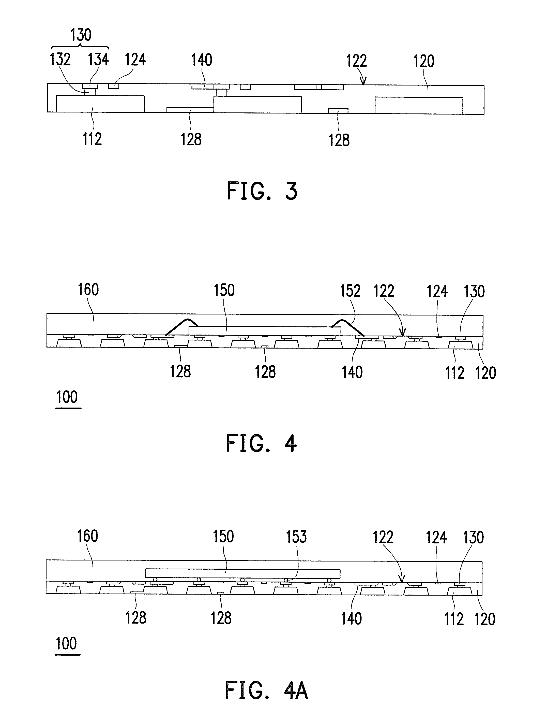
[0031]FIG. 1 is a schematic view of a lead frame according to an embodiment of the invention. FIG. 2 is a schematic view of a package structure according to an embodiment of the invention. FIG. 3 is a partial cross-sectional view of a package structure according to an embodiment of the invention. Referring to FIG. 1 to FIG. 3, the package structure 100 in the present embodiment includes a lead frame 110, a selective electroplating epoxy compound 120, a plurality of first conductive vias 130 and a first patterned circuit layer 140. The lead frame 110 as shown in FIG. 1 is firstly provided and includes a metal stud array having a plurality of metal studs 112 arranged in an array manner.
[0032]The lead f...
PUM
 Abstract
Description
Claims
Application Information