Packages for semiconductor devices and methods for assembling same

a technology of semiconductor devices and packaging, applied in the direction of fluid speed measurement, instruments, coatings, etc., can solve the problems of high processing cost, inability through vias, so as to reduce package thickness, reduce package thickness, and minimize the uppermost height of conductive wires

Active Publication Date: 2016-12-27
STMICROELECTRONICS INT NV
View PDF4 Cites 0 Cited by
  • Summary
  • Abstract
  • Description
  • Claims
  • Application Information

AI Technical Summary

Benefits of technology

[0010]In some embodiments, an end of the conductive wires are attached to a bond pad of the ASIC die in a way that minimizes the uppermost height of the conductive wire. In that regard, a third dimension (height) of package may be minimized. The package may thus be formed without utilizing through vias extending through either the ASIC die or the MEMS die. Through vias, although helpful at reducing package thickness, are expensive to process. Thus, one or more embodiments allow for thin packages at reasonable costs.
[0011]In some embodiments, the ASIC die may be offset on the surface of the MEMS die such that a portion of the ASIC die overhangs a surface of the MEMS die. Although this may increase one dimension of the package, at least one dimension of MEMS die defines a dimension of the package.

Problems solved by technology

Through vias, although helpful at reducing package thickness, are expensive to process.

Method used


Image

  • Packages for semiconductor devices and methods for assembling same
  • Packages for semiconductor devices and methods for assembling same
  • Packages for semiconductor devices and methods for assembling same

Examples


Embodiment Construction

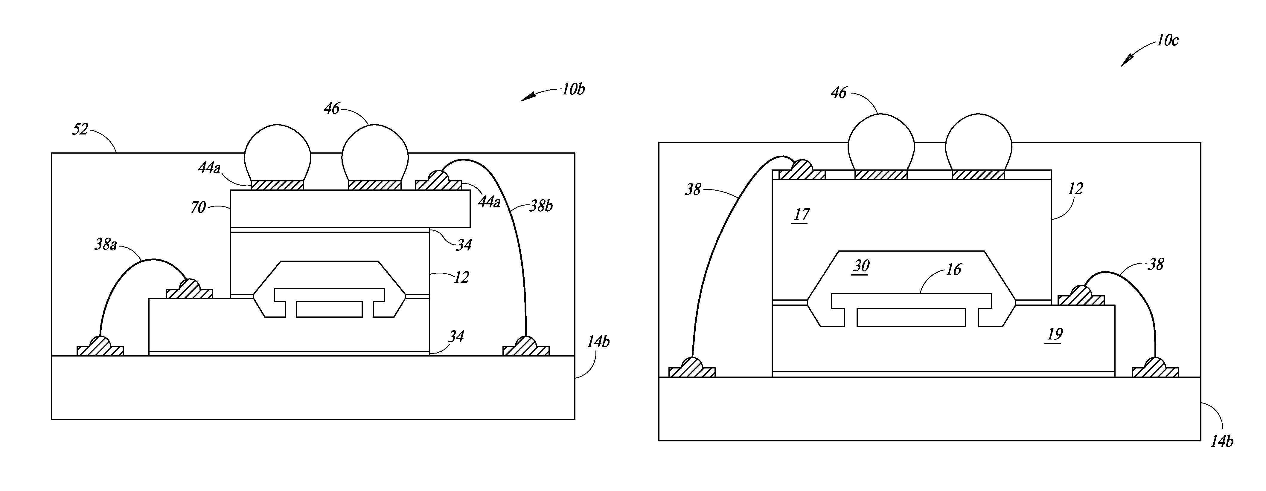
[0020]FIG. 1 shows a chip scale package 10 that includes a MEMS die 12 on an integrated device, such as an application-specific integrated circuit (ASIC) die 14 in accordance with one embodiment. In the illustrated embodiment, the ASIC die 14 is smaller than the MEMS die 12.

[0021]The MEMS die 12 includes a cap 20 and a substrate 22 that is secured to the cap 20 forming a cavity 30 therebetween. The cap 20 may be secured by any material suitable for securing the cap 20 to the substrate 22, such as glue, paste, or any other adhesive material.

[0022]The substrate 22 of the MEMS die 12 is formed from a semiconductor material, such as silicon, and integrates a moveable micro-electromechanical structure 16, such as a sensor, configured to detect an electrical parameter, such as capacitance or resistance. In particular, moveable micro-electromechanical structure 16 may include one or more beams, membranes, fingers, or other moveable structure are is configured to move in response one or mor...


PUM

PropertyMeasurementUnit
diameteraaaaaaaaaa
diameteraaaaaaaaaa
thickaaaaaaaaaa

Abstract

One or more embodiments of the present disclosure are directed to packages that include a stacked microelectromechanical sensor MEMS die and an application-specific integrated circuit (ASIC) die. The smaller of the MEMS die and the ASIC die is stacked on the larger of the MEMS die and the ASIC die. The larger of the two dice may form one or more dimensions of the package. In one embodiment, a bottom surface of the larger of the two dice forms an outer surface of the package. In that regard, the package may take less lateral space on another component, such as a board or other package.

Description

BACKGROUND[0001]Technical Field[0002]The present disclosure generally relates to the field of semiconductor packaging and methods for assembling same.[0003]Description of the Related Art[0004]Semiconductor die are packaged to protect the die from the external environment and to provide mechanical support. For manufacturers of semiconductor devices, there is a continuing pressure to increase the size of the packages. One response to this pressure has been the development of chip scale and wafer level packaging. These are packages that have a footprint that is very close to the actual area of the semiconductor die. Chip scale packages are generally direct surface mountable, using, e.g., ball grid arrays (BGA) and flip chip configurations.[0005]Another response has been to assemble system-in-packages (SiP), which include multiple semiconductor dice or chips enclosed in a single package body. For instance, micro-electromechanical systems (MEMS) packages often include a MEMS die and an a...

Claims


Application Information

Patent Timeline
Patent Type & Authority Patents(United States)
IPC IPC(8): B81C1/00B81B7/00
CPCB81C1/0023B81B7/0074B81C2203/0792H01L2224/48091H01L2224/48227H01L2224/48464H01L2224/73207H01L2224/73265H01L2224/94H01L2924/181H01L2924/00012H01L2924/00014B81C1/00238
Inventor CACHIA, CONRAD
Owner STMICROELECTRONICS INT NV
Why Eureka
Try Eureka