Ion guide

a technology of ion guides and ion channels, which is applied in the direction of microminiaturised spectromotors, electric discharge tubes, particle separator tubes, etc., can solve the problems of insufficient depth of potential, inability to provide an effective way to construct ion guides, and numerous design challenges, so as to increase the tracking distance between adjacent electrodes and increase the shadowing effect of the open dielectric surfa

Active Publication Date: 2017-01-03
THERMO FISHER SCI BREMEN
View PDF7 Cites 6 Cited by
  • Summary
  • Abstract
  • Description
  • Claims
  • Application Information

AI Technical Summary

Benefits of technology

[0011]The invention provides an ion guide that enables RF guiding of ions accompanied by much reduced charging-up of dielectric surfaces. The metal electrodes are arranged with respect to the dielectric surfaces in such a way that ions and / or droplets tend to fall only on the metal surfaces, which are biased in use, and not on dielectric surfaces. The planar design enables embodiments that have a reduced amount of collisions of neutral species with the electrodes. The design also enables embodiments that enable effective separation of neutral species from ions. The ion guide may be manufactured in a simple manner due to the planar electrode construction and the ability to use planar dielectric materials such as printed circuit board. The design may be realised in embodiments permitting filling of the ion guide with gas for collisional cooling or ion fragmentation. These and other advantages are described in more detail below.
[0015]An adjacent pair of electrodes on a planar dielectric surface are preferably arranged such that their ion-facing surfaces are at different distances, i.e. at different heights, from the surface of the dielectric material. Thus, the electrode of the pair with its ion-facing surface at the greater distance from the surface than the other is the electrode that overhangs the exposed portion of dielectric surface. This may also facilitate the overhanging of one electrode over at least part of an adjacent electrode and thereby even greater shadowing of the exposed portion of dielectric surface therebetween. Thus, the overhanging electrode preferably overhangs at least part of the other electrode of said adjacent pair of electrodes. Preferably, the overhanging electrode is an RF electrode. Thus, in such embodiments, the RF electrode may be the electrode that has an ion-facing surface at a greater distance or height from the dielectric surface to enable it to overhang.
[0027]In preferred embodiments, there is provided a first such electrode arrangement, i.e. as described herein, and there is a second such electrode arrangement spaced apart from the first such electrode arrangement, preferably parallel thereto. Preferably, the electrodes of the first such electrode arrangement face the electrodes of the second such electrode arrangement and the ion flow path is arranged between the first and second such electrode arrangements, preferably equidistant therebetween. The first and second such electrode arrangements in general may each comprise N RF electrodes with alternating RF phases (N=2, 3, 4 or higher), thereby forming a 2N polar multipole field (N=2 quadrupole, N=3 hexapole, N=4 octapole, etc.). Preferably, the first such electrode arrangement and the second such electrode arrangement together form a multipole electrode arrangement. Thus, each electrode arrangement is provided preferably on a separate piece of dielectric material such as a separate piece of circuit board material and each piece of dielectric material thereby carries one half of the electrodes of the whole multipole electrode arrangement. In one type of embodiment, the gap between the first and second such electrode arrangements is preferably at least 1 mm, or at least 3 mm, or at least 5 mm. Most preferably, the gap is 2 to 10 mm. However, the ion guide could be scaled up or down in size by at least an order of magnitude to suit the required application. For example, miniaturisation could enable the ion guide to be fabricated as a micro system device. In general, the gap between the first and second such electrode arrangements is about 2 to 3 times larger than the height of the ion beam that travels along the ion path in use. The exposed portion of dielectric surface between electrodes may be in the form of said one or more grooves, i.e. with the groove being formed in the portion of dielectric surface between the adjacent electrodes. There may be provided one or more grooves between each RF electrode and an electrode adjacent thereto (e.g. DC electrode). This increases the tracking distance between adjacent electrodes and increases the shadowing of the open dielectric surface.

Problems solved by technology

However, the design of such devices presents numerous challenges.
Such constructions are typically formed using conventional machining methods and invariably require cumbersome assembly and numerous parts.
However, this approach has the disadvantage of not providing an effective way to construct an ion guide with a deep enough potential well for use in mass spectrometry.
Other disadvantages of the foregoing designs include not providing a robust construction that could also be used to confine gas for collisional cooling of ions for example, and charging up of dielectric gaps between electrodes that can affect ion motion.
Whilst there are designs without dielectric (e.g. using resistive rods to generate a gradient field), such designs are difficult to manufacture.
For conventional multipoles positioned near to the ion source, a large amount of neutral species also typically collide with the multipole rods, which again can affect performance over time.

Method used


Image

  • Ion guide
  • Ion guide
  • Ion guide

Examples


Embodiment Construction

[0038]In order to assist further understanding of the invention, but without limiting the scope thereof, various exemplary embodiments of the invention are described below with reference to the Figures.

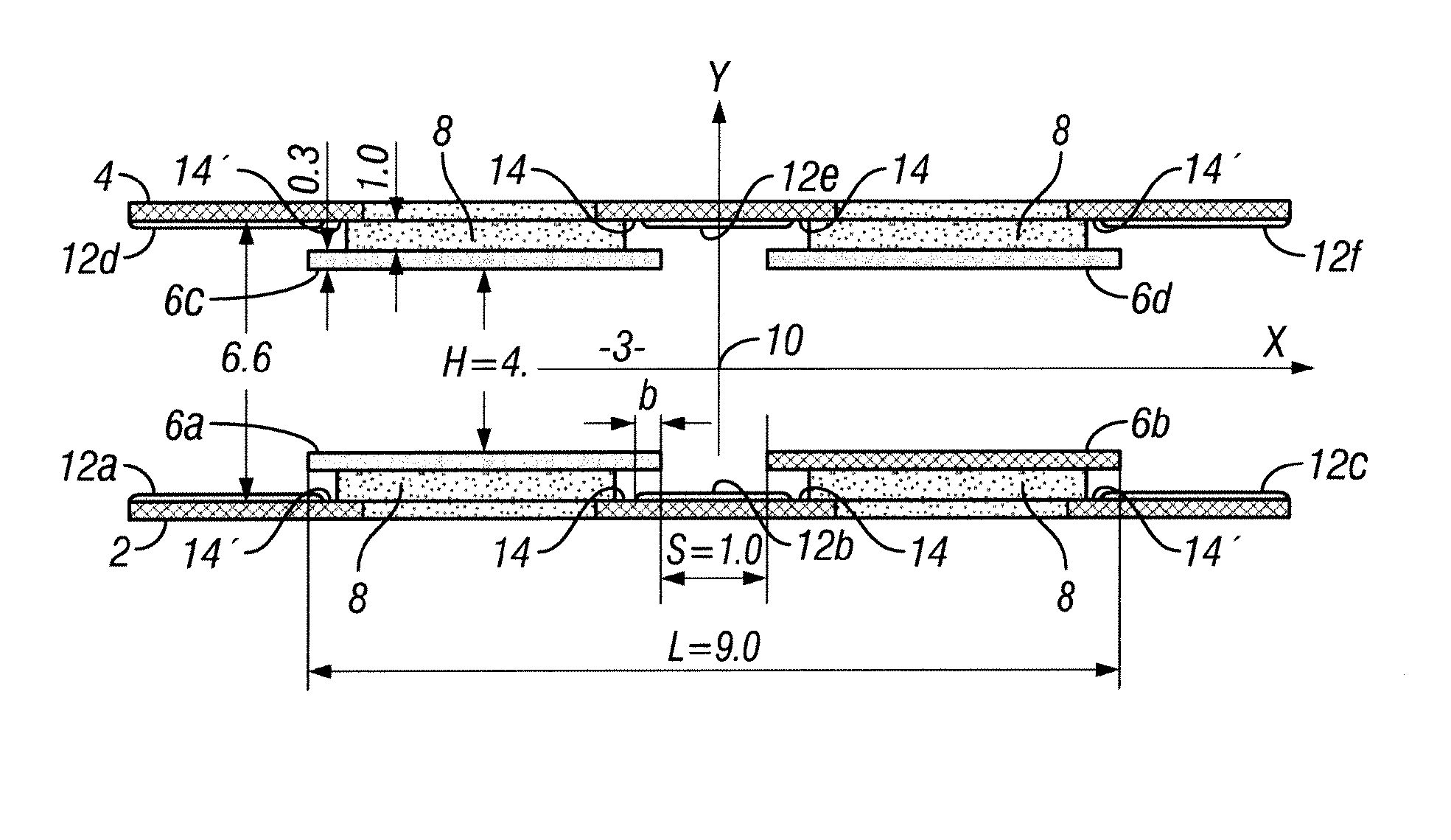
[0039]Referring to FIG. 1, there is shown a schematic sectional view of an embodiment of an RF ion guide according to the invention, with examples of dimensions in millimeters (mm) indicated. The ion guide comprises a first planar printed circuit board (PCB) (2) and spaced apart therefrom a second planar PCB (4). A space (3) thus exists between the PCBs. The PCBs (2) and (4) are arranged with the planes of the PCBs parallel to each other and facing each other. In the Figure, the planes of the PCBs extend perpendicular to the plane of the drawing, i.e. in the X-Z plane (the Z-axis running out of the plane of the drawing, parallel to the plane of the PCBs). The axis X is shown in the plane of the drawing, parallel to the plane of the PCBs and the axis Y is shown in the plane of the draw...


PUM


Abstract

An ion guide for mass spectrometry comprising an electrode arrangement of at least two electrodes, at least one of which is an RF electrode, arranged adjacent to each other but spaced apart on a planar surface of a dielectric material and arranged at a distance from an ion flow path, wherein a portion of the dielectric surface is exposed between an adjacent pair of the spaced apart electrodes and wherein at least one electrode of said adjacent pair of electrodes is arranged to overhang the exposed portion of surface between them such that there is no direct line of sight from the ion flow path to the exposed portion of dielectric surface. The device enables RF guiding of ions accompanied by much reduced charging-up of dielectric surfaces and reduced amount of collisions of neutral species with electrodes.

Description

FIELD OF THE INVENTION[0001]This invention generally relates to ion guides for use in mass spectrometry.BACKGROUND OF THE INVENTION[0002]RF ion guides, such as RF multipoles, are widely used in mass spectrometry in ion optical devices. Examples of devices comprising RF ion guides include mass filters, collision cells, ion traps and transport multipoles. However, the design of such devices presents numerous challenges.[0003]In recent years, RF ion guides with additional axial fields have been developed for better control of ion motion, for example as disclosed in U.S. Pat. No. 5,847,386, U.S. Pat. No. 6,111,250, EP1271611, U.S. Pat. No. 6,674,071, U.S. Pat. No. 6,107,628, U.S. Pat. No. 7,164,125, U.S. Pat. No. 7,064,322 and U.S. Pat. No. 7,564,025. These ion guides typically consist of massive metal or resistive RF rods, usually of circular section, and different means to provide an additional DC distribution along the axis of the guide. Such constructions are typically formed using ...

Claims


Application Information

Patent Timeline
Patent Type & Authority Patents(United States)
IPC IPC(8): H01J49/06H01J49/00H05K1/02
CPCH01J49/063H01J49/0018H01J49/062H01J49/068H05K1/02H01J49/4255
Inventor GRINFELD, DMITRYHAUSCHILD, JAN-PETERBALSCHUN, WILKODENISOV, EDUARDMAKAROV, ALEXANDER
Owner THERMO FISHER SCI BREMEN
Why Eureka
Try Eureka