Methods for fabricating programmable devices and related structures

Inactive Publication Date: 2017-02-07
GLOBALFOUNDRIES INC
View PDF12 Cites 1 Cited by
  • Summary
  • Abstract
  • Description
  • Claims
  • Application Information

AI Technical Summary

Benefits of technology

This patent describes a method and structure for making a programmable device by forming openings in a layer of a circuit structure, adding a material to catalyze the growth of nanowires or nanotubes in the openings, and then adding a dielectric material to surround the nanowires or nanotubes. This method and structure provide advantages over previous methods and can be used to create programmable devices with improved performance.

Problems solved by technology

As CMOS technology continues to shrink, new transistor feature designs such as FinFETs based on gate-last flow (or replacement gate flow) have been integrated into circuit structure so that the poly-Si gate serves as “dummy” gate and is no longer available.
Such an e-fuse is not suitable for on-chip programming on field (after chip packaged and tested) by using battery power.

Method used


Image

  • Methods for fabricating programmable devices and related structures
  • Methods for fabricating programmable devices and related structures
  • Methods for fabricating programmable devices and related structures

Examples


Embodiment Construction

[0009]Aspects of the present invention and certain features, advantages, and details thereof, are explained more fully below with reference to the non-limiting examples illustrated in the accompanying drawings. Descriptions of well-known materials, fabrication tools, processing techniques, etc., are omitted so as not to unnecessarily obscure the invention in detail. It should be understood, however, that the detailed description and the specific examples, while indicating aspects of the invention, are given by way of illustration only, and are not by way of limitation. Various substitutions, modifications, additions, and / or arrangements, within the spirit and / or scope of the underlying inventive concepts will be apparent to those skilled in the art from this disclosure.

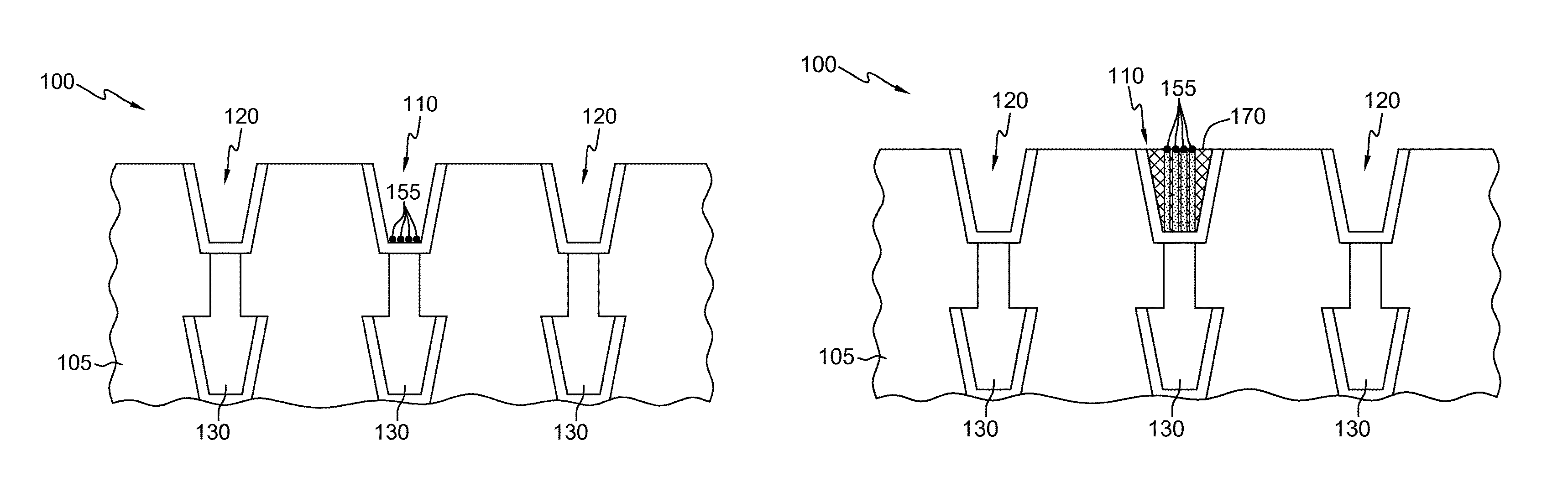
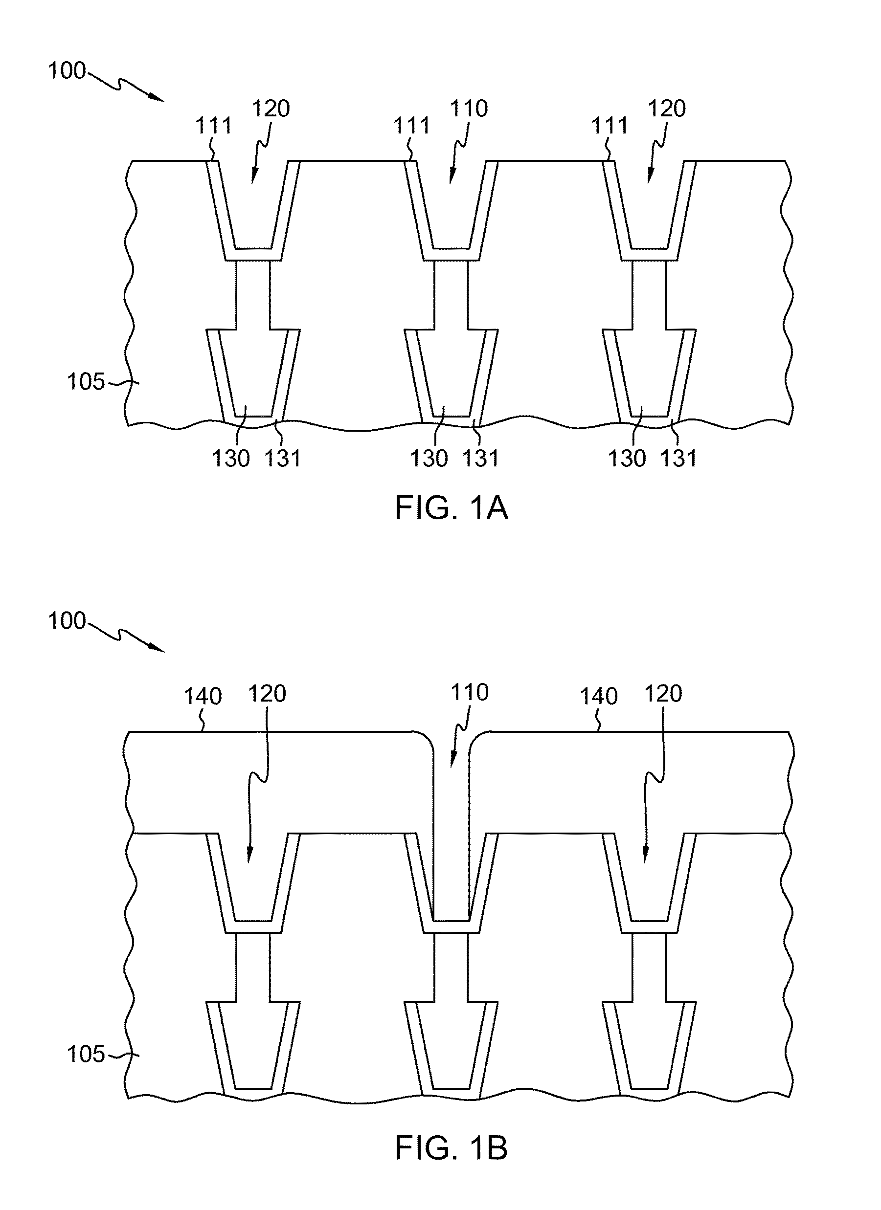
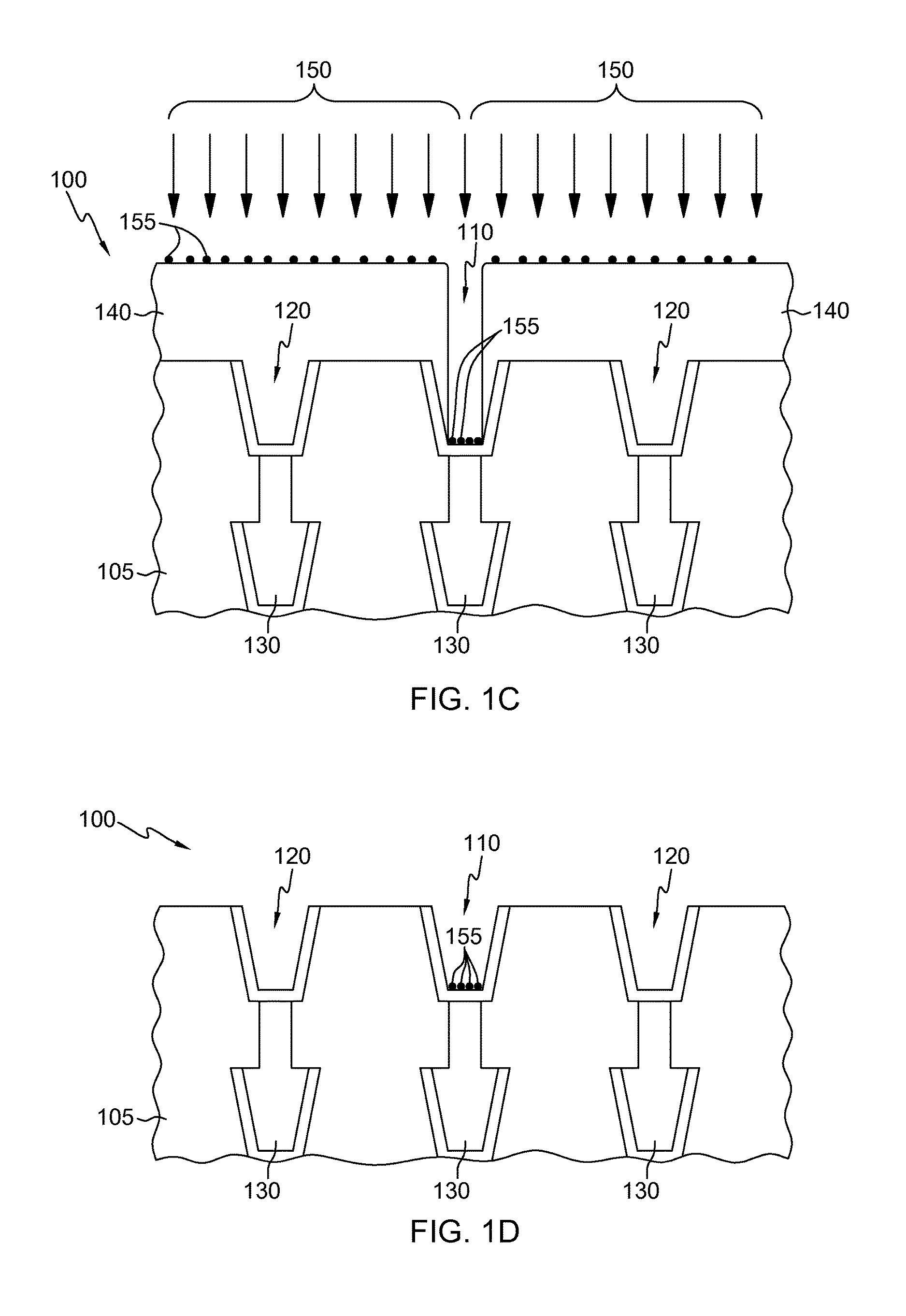
[0010]Many integrated circuits may include fuse structures or programmable devices that allow for customization of the circuit configuration during factory testing or by final users on field, generally through permane...


PUM


Abstract

Methods and structures for programmable device fabrication are provided. The methods for fabricating a programmable device include, for example forming at least one via opening in a layer of the programmable device and providing a catalyzing material over a lower surface of the at least one via opening; forming a plurality of nanowires or nanotubes in the at least one via opening using the catalyzing material as a catalyst for the forming of the plurality of nanowires or nanotubes; and providing a dielectric material in the at least one via opening so that the dielectric material surrounds the plurality of nanowires or nanotubes. The programmable device may, in subsequent or separate programming steps, have programming of the programmable device made permanent via thermal oxidation of the dielectric material and the plurality of nanowires or nanotubes, leaving a non-conducting material behind in the at least one via opening.

Description

FIELD OF THE INVENTION[0001]The present invention generally relates to fabricating a programmable device, and more specifically to methods of forming a one-time programmable (OTP) device that include forming a plurality of nanowires or nanotubes in a via opening using a catalyzing material.BACKGROUND[0002]Many integrated circuit structures may include structures or devices, often referred to as electrically programmable fuses or “e-fuses,” that enable permanent programming of some portion of the integrated circuit structure. Electrically programmable fuses may be programmed by “blow-out” of the fuse to make that portion of the circuit structure electrically “open,” such that once e-fuse programming is completed electric current may no longer flow through the e-fuse, and the programming of the e-fuse is one-time and non-reversible or permanent. In earlier nodes of technology (e.g. 90 nm or greater), the e-fuse is frequently made by poly-Si or silicided poly-Si fabricated at same time...

Claims


Application Information

Patent Timeline
IPC IPC(8): H01L27/112G11C13/00
CPCH01L27/11206G11C13/0002G11C13/0009H01L27/112G11C13/0069G11C13/025G11C2013/008H01L29/0676H01L29/413H01L23/5256H01L23/53276H10B20/25H10B20/20H10B20/00
Inventor PATIL, SURAJ K.JACOB, AJEY P.CHI, MIN-HWA
Owner GLOBALFOUNDRIES INC
Why Eureka
Try Eureka