
Circuitry and method for measuring negative bias temperature instability (NBTI) and hot carrier injection (HCI) aging effects using edge sensitive sampling

a technology of temperature instability and sampling method, applied in the field of on-chip aging compensation, can solve the problems of ic's finite lifetime, aging effects may become more pronounced, wear or aging can occur,

Inactive Publication Date: 2017-02-07
QUALCOMM INC
View PDF6 Cites 14 Cited by
  • Summary
  • Abstract
  • Description
  • Claims
  • Application Information

AI Technical Summary

Benefits of technology

This patent is about improving the performance and lifespan of semiconductor devices by compensating for aging and wear. The invention relates to using sensors and accelerating wear on dummy paths to measure the actual critical paths and adjust other sensors on the chip accordingly. This helps to account for process variations and wear and tear, resulting in better performance and reliability of the chip.

Problems solved by technology

While Integrated Circuit (IC) semiconductor devices are much more stable over time compared with older technologies, signs of wear or aging can occur, and IC's can have a finite lifetime.
As device sizes shrink, aging effects may become more pronounced.
These “hot” electrons can damage the gate oxide, resulting in trapped charges.
As more charges are trapped over the lifetime of a chip, the transistor threshold voltages may increase, reducing the transistor's current drive and speed.
NBTI may have a greater impact on p-channel transistors than on n-channel transistors, resulting in circuit skews.
Other mechanisms that cause circuit wear may also exist or are yet to be discovered and understood.
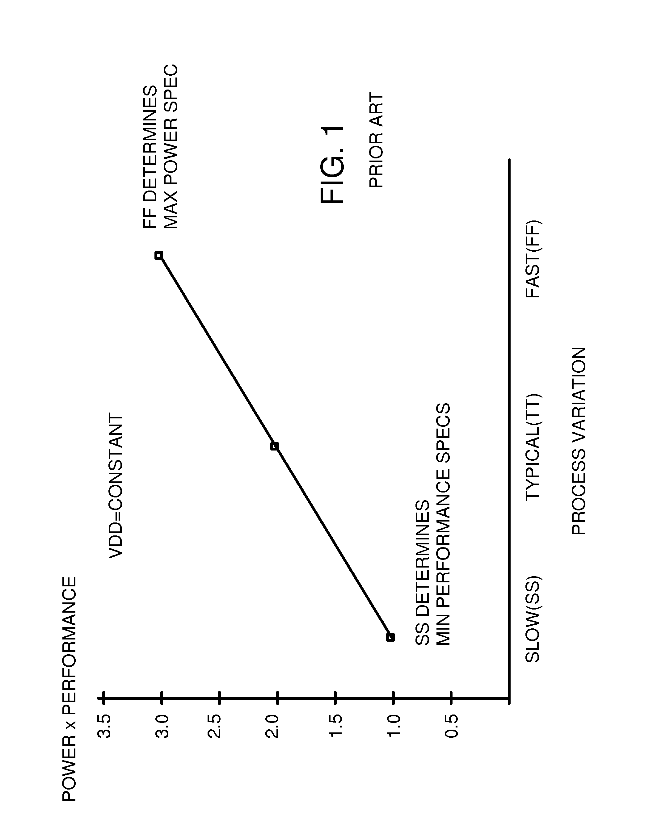
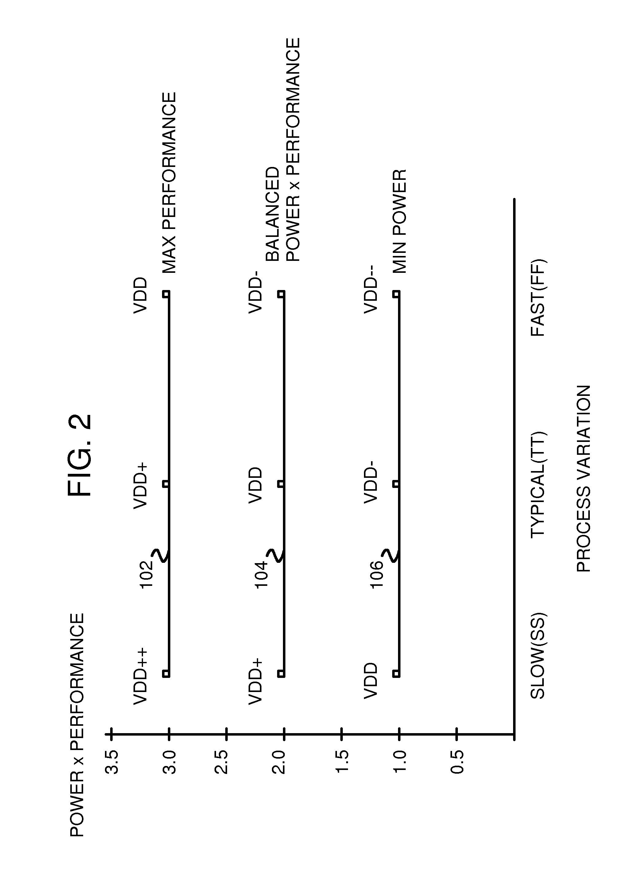
Although the manufacturing process may target a typical device, sometimes process variations produce slower chips or faster chips.
Unfortunately, such process skews are not always reproducible or planned but may occur randomly, making for logistical difficulties.
The fastest process skew (FF) has the highest performance and speed, but also consumes the most power.
This is not optimal, since fast devices are spec'ed slower than they can actually operate, and slow devices actually draw less power than spec'ed.
Also, as the devices age, wear occurs, such as by HCI or NBTI.
This wear may be caused by trapped electrons or other ions that gradually increase threshold voltages and thus reduce current drive.
As thresholds gradually rise over the life of the chip, the chip's performance worsens.
However, the actual circuit may be much more complex than an oscillator, resulting in tracking errors.

Method used


Image

  • Circuitry and method for measuring negative bias temperature instability (NBTI) and hot carrier injection (HCI) aging effects using edge sensitive sampling
  • Circuitry and method for measuring negative bias temperature instability (NBTI) and hot carrier injection (HCI) aging effects using edge sensitive sampling
  • Circuitry and method for measuring negative bias temperature instability (NBTI) and hot carrier injection (HCI) aging effects using edge sensitive sampling

Examples


Embodiment Construction

[0026]The present invention relates to an improvement in wear sensors. The following description is presented to enable one of ordinary skill in the art to make and use the invention as provided in the context of a particular application and its requirements. Various modifications to the preferred embodiment will be apparent to those with skill in the art, and the general principles defined herein may be applied to other embodiments. Therefore, the present invention is not intended to be limited to the particular embodiments shown and described, but is to be accorded the widest scope consistent with the principles and novel features herein disclosed.

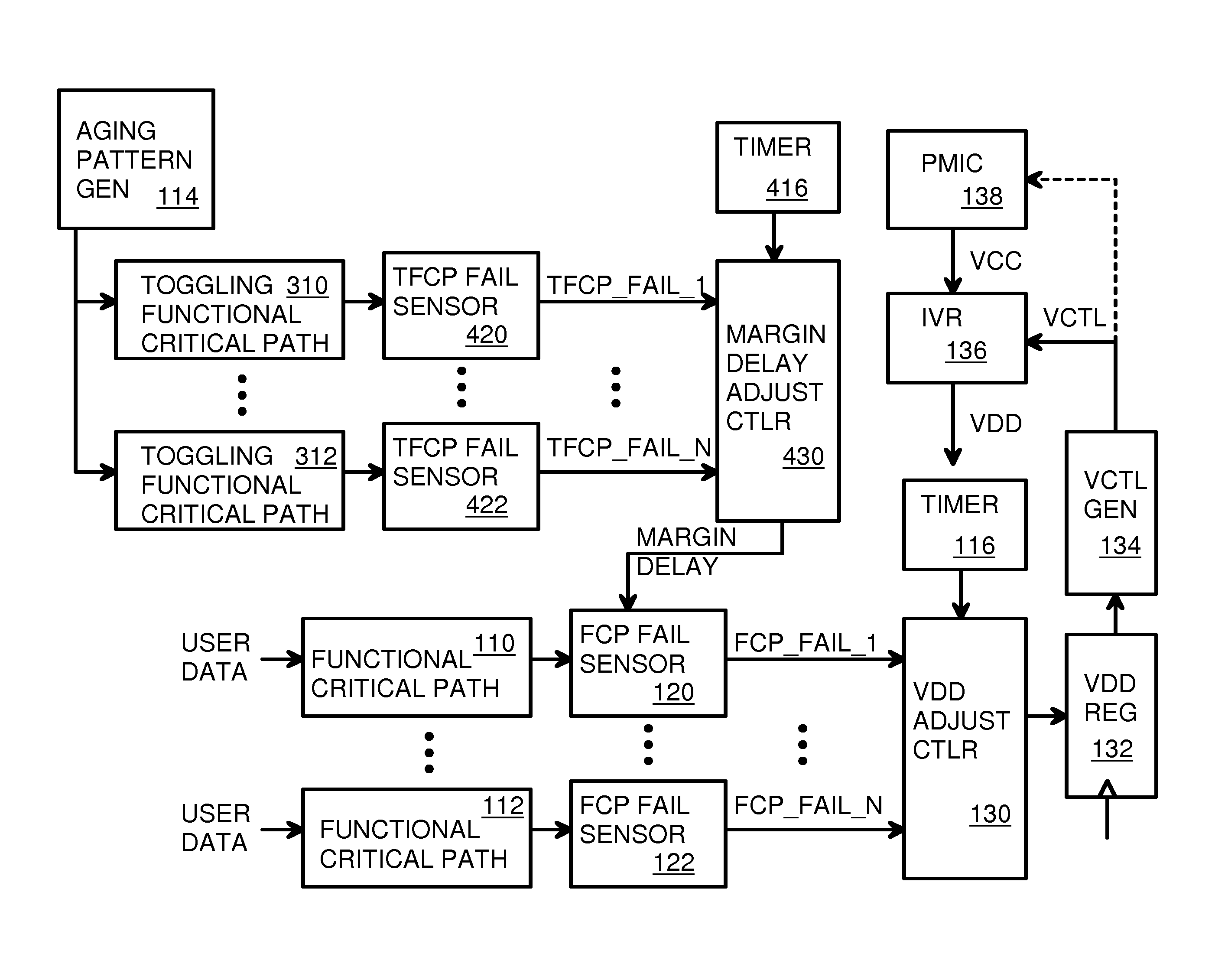
[0027]The inventors realize that test data patterns that accelerate wear can be applied to a dummy path, and the slowing of that dummy path over its lifetime can be measured. The measured wear can then be used to adjust added timing margins in other sensors on the chip. The added timing margin accounts for the actual wear measured.

[0028]...


PUM


Abstract

Toggling functional critical path timing sensors measure delays in toggling functional critical paths that continuously receive patterns from an aging pattern generator. Wear is accelerated. A margin delay adjustment controller sweeps margin delays until failures occur to measure delays. The margin delay is then adjusted in functional critical path timing sensors that add the margin delay to functional critical paths that carry user data or chip controls during normal operation. When the path delays fail to meet requirements, the functional critical path timing sensors signal a controller to increase VDD. When no failures occur over a period of time, the controller decreases VDD. Wear on the toggling functional critical paths is accelerated using both toggle and low-transition-density patterns. Circuit aging is compensated for by increasing margin delays to timing sensors.

Description

RELATED APPLICATION[0001]This application is a non-provisional of the provisional application for “Circuitry and Method for Critical Path Timing Speculation using Edge Sensitive Sampling”. U.S. Ser. No. 62 / 146,412, filed Apr. 13, 2015.FIELD OF THE INVENTION[0002]This invention relates to on-chip aging compensation, and more particularly to accelerating wear of critical paths and using sensed delays to adjust other sensors in a chip.BACKGROUND OF THE INVENTION[0003]While Integrated Circuit (IC) semiconductor devices are much more stable over time compared with older technologies, signs of wear or aging can occur, and IC's can have a finite lifetime. As device sizes shrink, aging effects may become more pronounced. For example, some newer flash memories may spec a reduced number of lifetime read / write cycles.[0004]Hot Carrier Injection (HCI) occurs when electrons are accelerated by a high electric field, such as near the drain of a Metal-Oxide-Semiconductor Field-Effect Transistor (MO...

Claims


Application Information

Patent Timeline
IPC IPC(8): G06F1/10H03K5/13H03K5/00
CPCH03K5/13H03K2005/00019G01R31/2858H03K3/0375
Inventor QUINTON, BRADLEYMCCLEMENTS, TRENTHUGHES, ANDREWTANEJA, SANJIV
Owner QUALCOMM INC
Learn More