High quantum efficiency photodetector

a photodetector and quantum efficiency technology, applied in the field of semiconductor photodetectors, can solve the problems of more or less arising problems, low quantum and low efficiency of such photodetectors

Active Publication Date: 2017-05-02
COMMISSARIAT A LENERGIE ATOMIQUE ET AUX ENERGIES ALTERNATIVES +1
View PDF5 Cites 25 Cited by
  • Summary
  • Abstract
  • Description
  • Claims
  • Application Information

AI Technical Summary

Problems solved by technology

Thus, the quantum efficiency of such photodetectors is low.
The problem is that layer 10 is, in modern technologies, very thin, typically with a thickness in the range from 1 to 1.5 μm.
Thus, a problem arises to absorb the maximum possible number of photons in photodetectors of small dimensions such as those shown in FIG. 1, and in photodetectors where the semiconductor layer for converting photons into electron-hole pairs is thin, such as that shown in FIG. 2.
More generally, this problem arises more or less in all semiconductor photodetectors.

Method used


Image

  • High quantum efficiency photodetector
  • High quantum efficiency photodetector
  • High quantum efficiency photodetector

Examples


Embodiment Construction

[0024]The same elements have been designated with the same reference numerals in the different drawings and, further, the various drawings are not to scale. In the following description, when reference is made to terms qualifying absolute positions, such as terms “front”, “rear”, “top”, “bottom”, “left”, “right”, etc., or relative positions, such as terms “above”, “under”, “upper”, “lower”, “lateral”, etc., or to terms qualifying directions, such as terms “horizontal”, “vertical”, etc., it is referred to the orientation of the drawings, it being understood that, in practice, the described photodetectors may be oriented differently. Unless otherwise specified, expressions “approximately”, “substantially”, and “in the order of” mean to within 10%, preferably to within 5%.

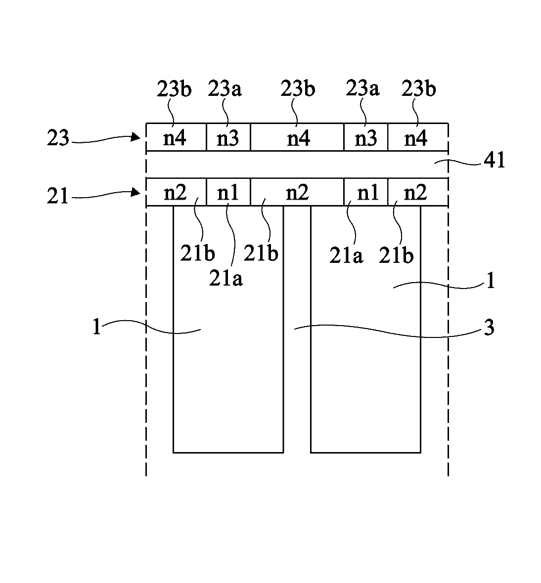
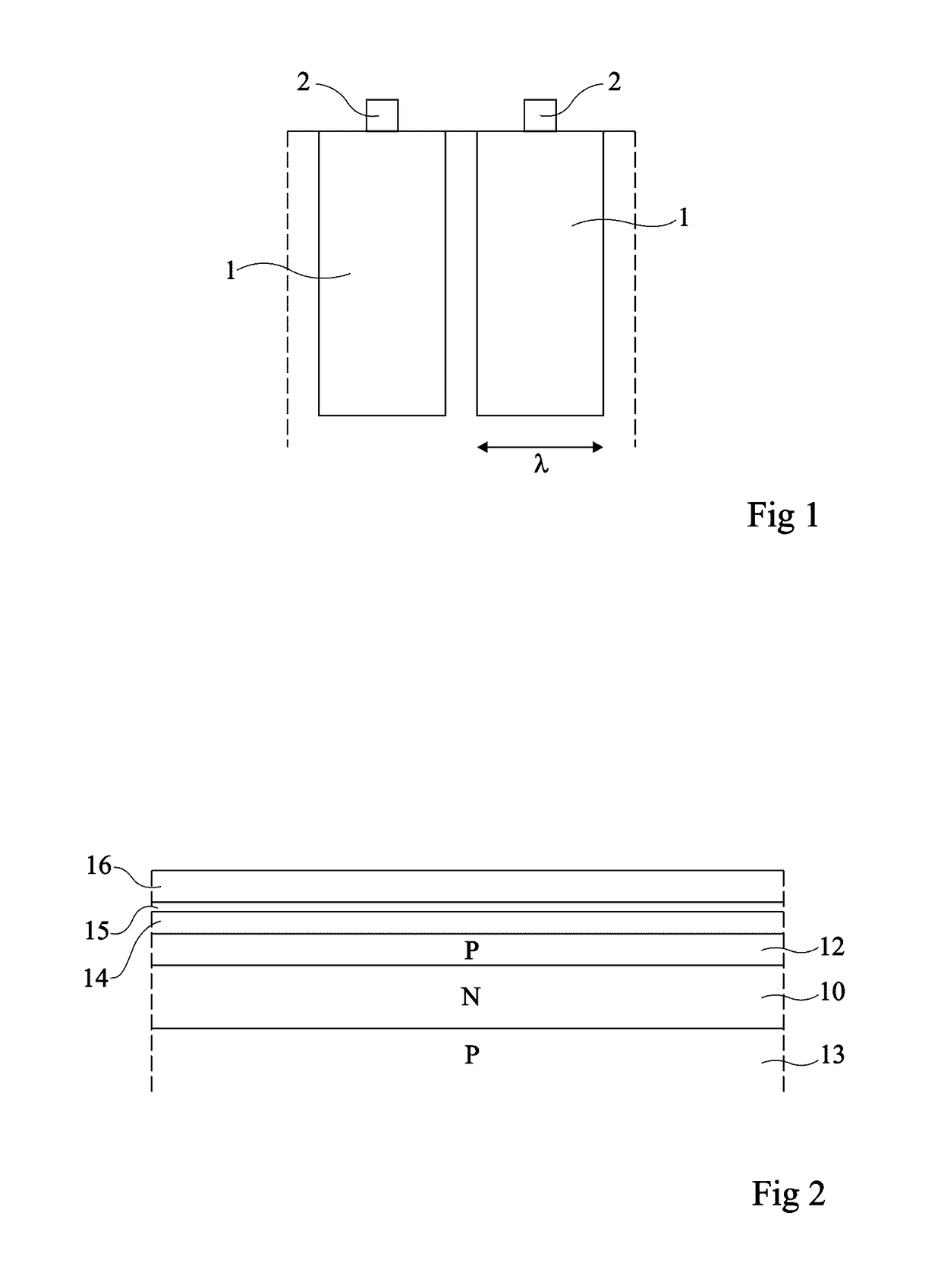
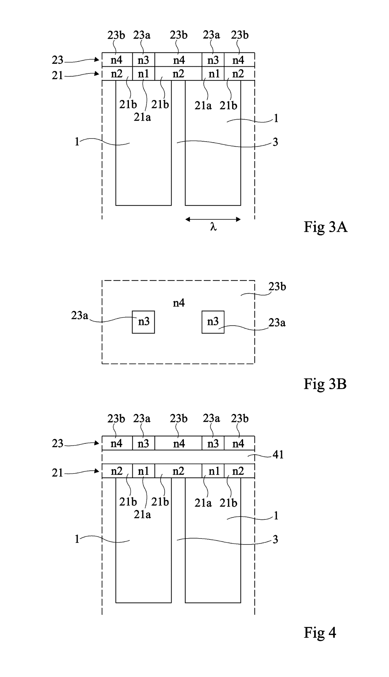
[0025]FIGS. 3A and 3B partially and schematically show an embodiment of two photodetectors side by side of an assembly of photodetectors, for example forming an image sensor. As in the example of FIG. 1, each photodet...


PUM


Abstract

A photodetector including a photoelectric conversion structure made of a semiconductor material and, on a light-receiving surface of the conversion structure, a stack of first and second diffractive elements, the second element being above the first element, wherein: the first element includes at least one pad made of a material having an optical index n1, laterally surrounded with a region made of a material having an optical index n2 different from n1; the second element includes at least one pad made of a material having an optical index n3, laterally surrounded with a region made of a material having an optical index n4 different from n3; the pads of the first and second elements are substantially vertically aligned; and optical index differences n1−n2 and n3−n4 have opposite signs.

Description

CROSS-REFERENCE TO RELATED APPLICATION[0001]This application claims the priority benefit of French Patent Application number 15 / 54878, which is hereby incorporated by reference in its entirety to the maximum extent allowable by law.BACKGROUND[0002]The present disclosure relates to semiconductor photodetectors, and more particularly to photodiode-type photodetectors, for example used as pixels of an image sensor, or as single-photon avalanche diodes.DISCUSSION OF THE RELATED ART[0003]FIG. 1 partially and schematically shows two photodetectors side by side of an assembly of photodetectors, for example forming an image sensor. Each photodetector comprises a semiconductor structure 1 for converting photons into electron-hole pairs. Structure 1 may comprise junctions (not shown) between semiconductor regions of opposite conductivity types to store the photogenerated electrons. In a complete photodetector, there further exist one or a plurality of read transistors (not shown) to transfer ...

Claims


Application Information

Patent Timeline
Patent Type & Authority Patents(United States)
IPC IPC(8): H01L29/49H01L31/107H01L27/146H01L31/0232H01L31/113
CPCH01L31/1133H01L27/14603H01L27/14643H01L31/02327H01L31/107
Inventor FREY, LAURENTMARTY, MICHEL
Owner COMMISSARIAT A LENERGIE ATOMIQUE ET AUX ENERGIES ALTERNATIVES
Why Eureka
Try Eureka