Top-emission organic electroluminescence display device and production method therefor

a display device and organic technology, applied in the direction of organic semiconductor devices, semiconductor devices, electrical devices, etc., can solve the problems of limited aperture ratio, uniform brightness, deterioration of light-emitting efficiency, etc., and achieve the effect of suppressing the deterioration of display characteristics

Active Publication Date: 2017-07-04
DAI NIPPON PRINTING CO LTD
View PDF39 Cites 0 Cited by
  • Summary
  • Abstract
  • Description
  • Claims
  • Application Information

AI Technical Summary

Benefits of technology

[0023]In an embodiment of the present invention, through the processes of: first, allowing the cover member to be in contact with the insulating layer between the areas where the contact portions are to be formed and the pixel electrodes adjacent to the areas under a first pressure and setting the space between the organic EL layer side substrate, in which the pixel electrodes, the auxiliary electrodes, the insulating layer, and the organic EL layer are formed on the substrate, and the cover member to be in a reduced pressure state; next, allowing the organic EL layer side substrate and the cover member to be adhered to each other by adjusting the space of the side of the cover member opposite to the organic EL layer side substrate to have a second pressure; and after that, removing the organic layer covering the auxiliary electrode exposed from the opening of the insulating layer by illuminating with a laser beam in order to form the contact portion; the organic layer removed by the laser beam can be sufficiently prevented from being scattered into the pixel areas, so that it is possible to obtain the effect that deterioration in display characteristics can be suppressed.
[0024]Incidentally, as a pressure for the “first pressure” and the “second pressure”, it is not particularly limited if the first pressure is a lower pressure than the second pressure. In addition, any pressures to the extent that, when adjusting the pressure of the space between the organic EL layer side substrate and the cover member at the time of arranging the cover member on the surface of the organic EL layer side substrate to be the first pressure and adjusting the pressure of the space of the side of the cover member opposite to the organic EL layer side substrate to the second pressure, the organic EL layer side substrate and the cover member can be adhered to each other by a pressure difference between the pressure between the organic EL layer side substrate and the cover member and the pressure of the space of the side of the cover member opposite to the organic EL layer side substrate may be employed without particular limitation. Incidentally, in general, the “first pressure” is set to a pressure lower than a normal pressure, and the “second pressure” is set to a pressure higher than the “first pressure”. In addition, since the “first pressure” is described in the later-described Section “B. Production Method for Organic EL Display Device”, the description thereof is omitted herein.

Problems solved by technology

Here, in the case of the active matrix driving organic EL display device, in the bottom emission type, there is a problem in that an aperture ratio is limited by the circuit such as TFT formed on the substrate, which is a light emitting surface, and a light emitting efficiency is deteriorated.
For this reason, in the organic EL display device having the transparent electrode layer, voltage drop occurs due to the resistance of the transparent electrode layer, and as a result, uniformity of brightness of the organic EL layer is deteriorated, so that a problem of so-called brightness irregularity occurs.
In addition, as an area of the transparent electrode layer is increased, the resistance is increased, and thus, the above-described problem of brightness irregularity becomes remarkable in the case of producing a large-sized display.
For this reason, in the top-emission organic EL display device, in the case where the auxiliary electrodes are formed after formation of the organic EL layer, there is a problem in that an etchant used for forming the auxiliary electrode is infiltrated into the organic EL layer.
However, in this case, the organic EL layer removed by the laser beam is scattered, and thus, pixel areas of the organic EL display device are contaminated, so that there is a problem in that display characteristics are deteriorated.
However, in this case, although the above-described deterioration in display characteristics can be suppressed, since the first electrode and the second electrode are formed as the transparent electrode layers, there is a problem in that the number of production processes is increased.

Method used


Image

  • Top-emission organic electroluminescence display device and production method therefor
  • Top-emission organic electroluminescence display device and production method therefor
  • Top-emission organic electroluminescence display device and production method therefor

Examples


example 1

[0195](Pixel Electrode / Auxiliary Electrode Forming Process)

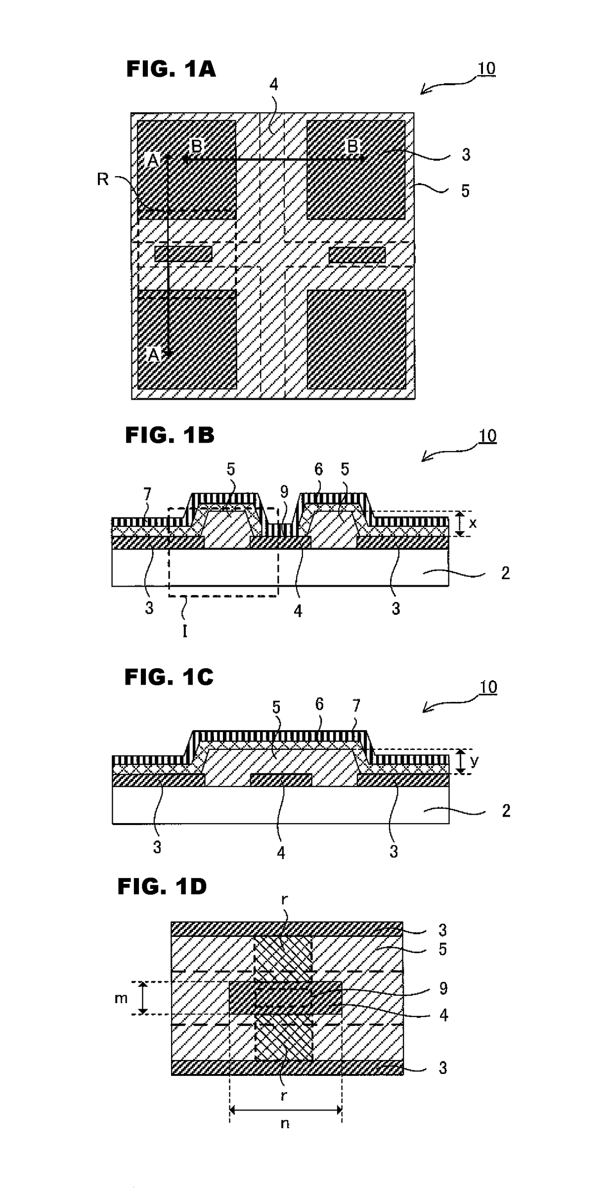
[0196]A chromium film having a thickness of 150 nm is formed on a substrate comprising an alkali-free glass having a thickness of 0.7 mm by a sputtering method. After that, pixel electrodes and auxiliary electrodes are simultaneously formed by a photolithography method.

[0197](Insulating Layer Forming Process)

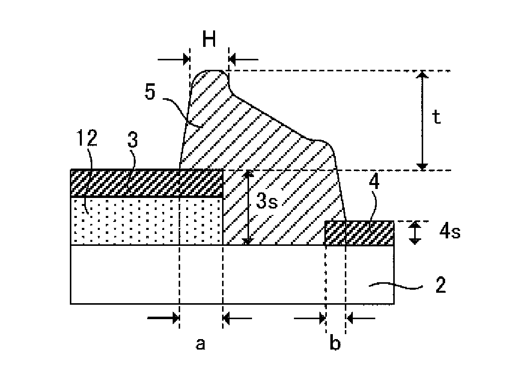
[0198]Next, an insulating layer is formed between the pixel electrodes to cover edge portions of, the adjacent pixel electrodes and to include openings exposing the auxiliary electrodes by a photolithography method. Incidentally, the longitudinal cross-sectional shape of the insulating layer is a forward tapered shape. In addition, when an overlap distance of the insulating layer between the contact portion and the pixel electrode adjacent to the contact portion with respect to the pixel electrode is regarded as “a” and an overlap distance of the insulating layer between the contact portion and the pixel electrode adjace...

example 2

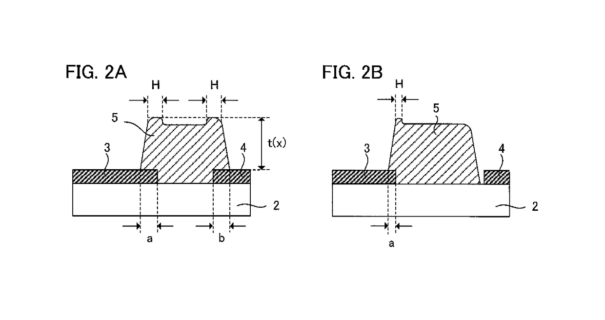
[0217]When the height of the insulating layer between the contact portion and the pixel electrode adjacent to the contact portion is regarded as “x” and the maximum height of the heights of the insulating layers other than the insulating layer between the contact portion and the pixel electrode adjacent to the contact portion is regarded as “y”, the organic EL display device is produced by the same method as that of Example 1 except that y−x is designed as listed in the following Table 3.

[0218]

TABLE 3y-xNo.(μm)50.260.170.0580.01

[0219](Evaluation)

[0220]The insulating layers are designed as Nos. 5 to 8 listed in Table 3, the space between the cover member and the organic EL layer side substrate is set to be in a reduced pressure state to adhere the organic EL layer side substrate and the cover member, and after that, the organic layers formed on the auxiliary electrodes are removed by the laser beam through the cover member. At this time, existence of the scattering of the organic lay...

example 3

[0224]The organic EL display device is produced by setting the same as Example 1 except that the organic EL layer forming process is performed as illustrated below.

[0225](Organic EL Layer Forming Process)

[0226]Next, a hole injecting layer and a hole transporting layer are formed on the pixel electrode so as to have a thickness of 0.1 μm and, after that, a light-emitting layer having 0.02 μm is formed on the hole transporting layer. After that, an electron transporting layer having a thickness of 0.03 μm is formed on the light-emitting layer, so that an organic EL layer is obtained. Incidentally, the organic EL layer is formed on the pixel electrode and is formed on the auxiliary electrode exposed from the opening of the insulating layer.

[0227](Evaluation)

[0228]The same result as that of Example 1 is obtained.


PUM


Abstract

A top-emission organic EL display device includes a substrate, pixel electrodes, auxiliary electrode, insulating layer formed between the pixel electrodes and includes an opening to expose the auxiliary electrode, organic EL layer formed on the pixel electrodes and includes organic layers, at least one formed on the auxiliary electrode, a contact portion being an opening of the organic layer formed on the auxiliary electrode, and transparent electrode layer formed on the organic EL layer and the contact portion. When an insulating layer overlap distance between the contact portion and pixel electrode adjacent to the contact portion with respect to the pixel electrode is regarded as “a” and an insulating layer overlap distance between the contact portion and pixel electrode adjacent to the contact portion with respect to the auxiliary electrode is regarded as “b”, at least one of “a” and “b” is equal to or greater than 2 μm.

Description

TECHNICAL FIELD[0001]The present disclosure relates to a top-emission organic electroluminescence display device including an auxiliary electrode.BACKGROUND ART[0002]Organic electroluminescence elements have drawn attention in terms of advantages such as high visibility by self-coloring, excellent, impact resistance for being an entirely solid display unlike a liquid crystal display device, a fast response rate, small influence by a change in temperature, and a wide viewing angle. Incidentally, hereinafter, in some cases, an organic electroluminescence is abbreviated to organic EL.[0003]The configuration of the organic EL element is based on a laminated structure where an organic EL layer is interposed between an anode and a cathode. As a driving method for the organic EL display device including the organic EL element, there are passive matrix driving and active matrix driving, but the active matrix driving is useful in terms that the active matrix driving can be performed at a low...

Claims


Application Information

Patent Timeline
Patent Type & Authority Patents(United States)
IPC IPC(8): H01L51/56H01L51/52H01L27/32
CPCH01L51/56H01L27/3246H01L27/3248H01L51/5212H01L51/5228H01L2251/5315H10K59/122H10K50/814H10K50/824H10K2102/3026H10K71/00H10K2101/00H10K59/123
Inventor NIRENGI, TAKAYOSHITAKEDA, TOSHIHIKO
Owner DAI NIPPON PRINTING CO LTD
Why Eureka
Try Eureka