

Method and device for measuring temperature during deposition of semiconductor
- Summary
- Abstract
- Description
- Claims
- Application Information
AI Technical Summary
Benefits of technology
Problems solved by technology
Method used
Image

Examples
Embodiment Construction
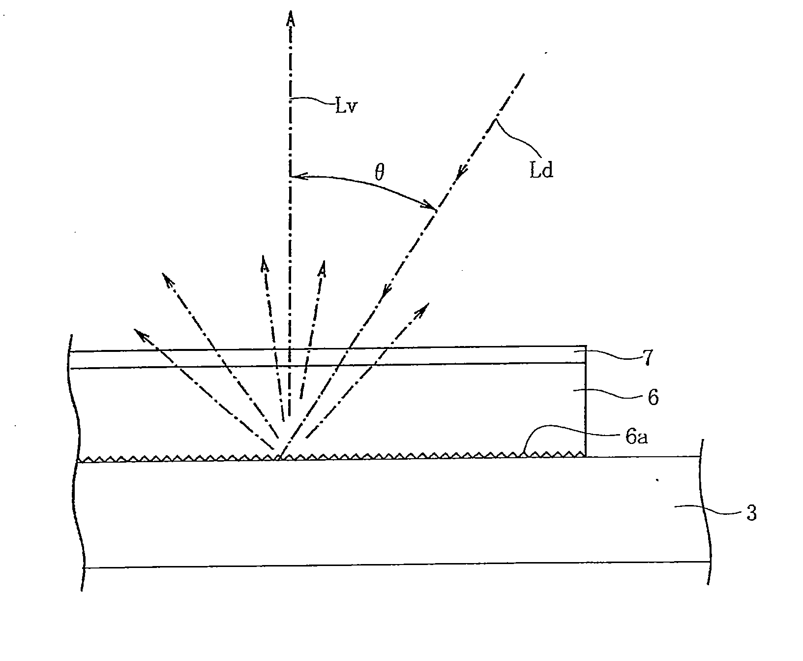
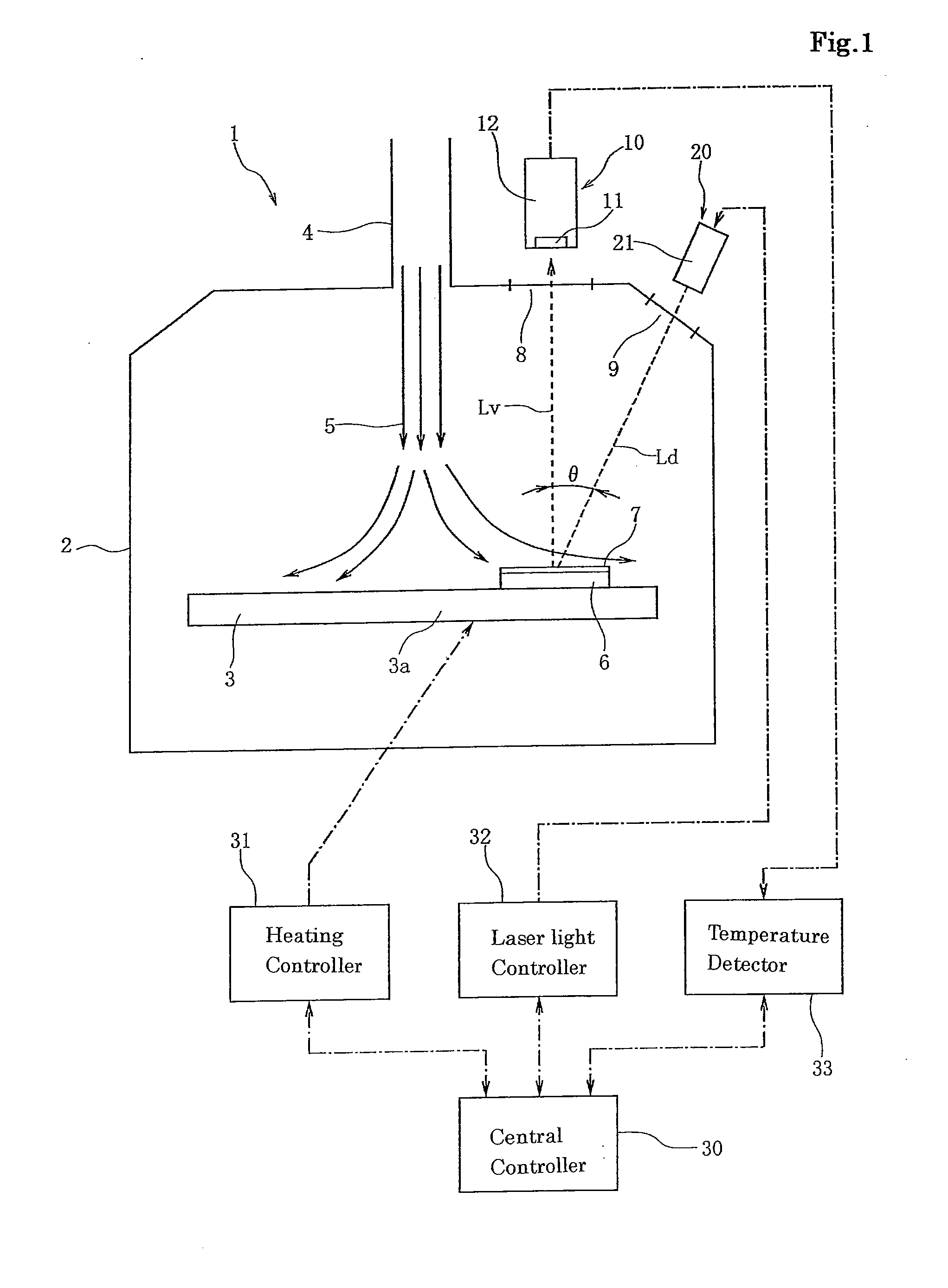
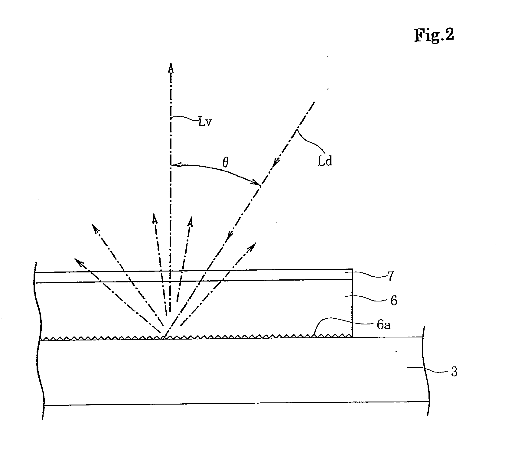
[0026]FIG. 1 is an explanatory drawing of the film deposition device and the temperature measuring device. FIG. 2 is a magnified explanatory drawing illustrating the substrate and semiconductor layer during deposition inside the film deposition device's chamber.
[0027]FIG. 1 shows a schematic diagram of the film deposition device 1 for a semiconductor layer by of chemical vapor deposition (CVD) or the molecular beam epitaxy (MBE) processes.
[0028]The film deposition device 1 is equipped with a chamber 2, the inside of which is maintained in reduced pressure state during film deposition. In the chamber 2, a table 3 is provided, wherein the heating system 3a is incorporated. The feed port 4 is connected to chamber 2, through which the source gas 5 including elements (source molecules) of film deposition for the semiconductor layer 7 is supplied to the surface of the table 3. The semiconductor layer 7 is deposited on the substrate 6 disposed on the table 3.
[0029]The chamber 2 is equipped...
PUM
| Property | Measurement | Unit |
|---|---|---|
| Temperature | aaaaa | aaaaa |
| Transmittivity | aaaaa | aaaaa |
Abstract
Description
Claims
Application Information